Scanning Electron Microscopy (SEM) Lecture: Principles, Techniques & Applications
59.08k views11096 WordsCopy TextShare
The Kavli Nanoscience Institute at Caltech
The KNI's Scanning Electron Microscopy lecture, presented by Matthew Sullivan Hunt, PhD (with an upd...
Video Transcript:
all right welcome my name is Matthew hunt I'm the staff microscopy here at the Kay and I the first of three lectures on microscopy over the next few weeks and scanning electron microscopy than gallium focused ion beam and then helium and neon focused ion beam okay so first of all I want to show an example of what it looks like to use a scanning electron microscope here we're going to scan the beam across a field of view that's 15 microns wide and we have patterned with metal K and I Caltech and some circles here so
this is silver it's got a lot of texture to it gold and titanium on silicon and so this is what's called the secondary electron image and we'll talk about what that means the secondary electron image is going to show us topography of the sample so as I start the video and the beam is scanning about once a second we're getting a refresh of the image here I'm about to change the voltage on a detector to take us from secondary electrons to what are called backscattered electrons and these are primarily going to give us atomic number
contrast so you can see the image changed dramatically and now I'm scanning at a slower rate so that now every five seconds we're capturing a new image and then I can go back to scanning a secondary electron image and now I'm back to more of a topographic image so throughout this lecture I'm going to explain all the different parts of this the voltage that we're using the current that we're using the working distance that we're using and lots of other tricks that we can employ to take nice images of all kinds of different features first
of all I'll say all of these resources including this presentation are available on our K&I lab wiki so that's kit lab k night at Cal Tech at IDI you can search for this quite easily so literally everything that you want to find resources related to microscopes you can find on our wiki this is just a slide to show the full functionality again there's a whole page that describes how you might choose a different microscope to use or which microscopes to use for your research in the K&I and this describes all the functionality these next three
lectures will be going through all these different things now you have handouts in front of you three of them for today that are relevant and then a fourth one and a fifth one for the different focused ion beams we're not going to go through it right now but as we go through the presentation you'll see these little diagrams appear on different slides and you'll have a way to follow along with your diagrams for the YouTube presentation I'll put links to them below the description of the video so there's SEM there's a handout on alignments and
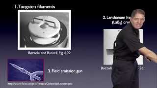
then there's also a handout considerations for optimizing your SEM images and we'll go through all these different things over the course of this presentation there are also books for each of these three types of microscopy that I'll go over these are the the notable books that I would recommend so look at those when you want to further study any of these concepts and what I'm gonna try to do over the course of these lectures is show the analogies between the three different types of microscopy and here's a good place to start these are the emission
sources and you'll see that each of them is a tungsten needle and will have some kind of extractor some kind of suppressor will have an accelerating voltage setup and we'll be able to draw analogy so they all look a little bit different and they have their own attributes that to give emission of electrons or gallium ions or helium ions they're all fundamentally of the same construction and so this will be a core concept of these lectures trying to draw analogies across the different microscope platforms so those were the sources the column optics again we'll see
that they're largely the same if we look at them in a cartoon diagram format we can see they have similar lenses they have similar stigmata or similar source construction and again that's what we're gonna use to ground ourselves and make sure that we understand how the analogies work across the different microscope platforms so before we start getting into the the physical concepts I'll just show some pictures of microscopes that we have in our lab which looks similar to microscopes in all the labs across the world so here is an SEM with the gallium focused ion
beam we call it a dual beam system in our lab so the SEM is on the main optical axis the gallium fib here is offset by 52 degrees here's a vacuum screen showing that we have things like ion getter pumps pumping on the columns and we have turbo molecular pump pumping on the chamber there's other things on here like we have an aperture controller I'll show what that looks like closer up later we have column isolation valve that's what keeps our columns isolated from the chamber when we're venting and I will show you I think
on the next slide what it looks like inside so when we open the door we vent the whole chamber in the case here we we could pull out the door and we see here's our specimen on a stub on a stub holder and an XYZ rotation tilt stage this is a six-inch stage our Nova 600 and we have the SEM column here we have a lot of other things inside the things that are relevant to us today are the Everhart Thornley detector and the through-the-lens detector these are secondary electron detectors I'll go through what it
means to create secondary electrons and detect them and why you would want to do that we have other things like gas injection system needles that would be important for our gallium focused ion beam presentation if we look at a reverse view we see other things here's the gallium column here's what's called an omni probe needle again those are things that will be more relevant for the next lecture we have some other things we have a magnetic field sensor so we can sense the magnetic field in near the column and then we can cancel that field
by running current through loops that are on three different walls of the room otherwise we'd get some oscillations in our beam and let's see otherwise some controllers I think that's those are the main things today for for SEM we have a nova 200 the 200 just means 2-inch stage so a lot of the same kind of stuff what's different here is we have a energy dispersive spectroscopy detector in a wavelength dispersive spectroscopy detector we'll talk about how we can use x-rays to analyze the elemental composition of our samples okay so when we talk about lenses
and when we get into the column optics we need to understand the difference between electromagnetic magnetic lenses which are used in electron systems and electrostatic lenses which we'll use in ion beam systems so the basic construction of an electromagnetic lens is what we have here so you have a wire coil like copper wire embedded in an iron shell and we run current through that wire so we generate a magnetic field and we allow an opening or a bore in that iron shell so this is radially symmetric so we leak that magnetic field out into the
opening of the or through into the column and as an electron beam passes through the electrons that are that are off axis will get bent strongly back towards the main axis because the field is stronger at the perimeter and those in the center won't get deflected at all in those that are say halfway between will get mildly deflected so the idea is we want to get to a crossover point or a focus point we'll talk about electrostatic lenses in the next lectures but they ultimately accomplish the same task through a different mechanism it's called an
ISO lens we have positive potential and then two other plates at ground potential these again think of them as concentric rings or plates and so we get we can symmetrically accelerate and decelerate the beam as it passes through the lens now another thing to mention with electrons in a magnetic field they spiral so this is kind of a very reduced cartoon version of what's happening but in cross-section you can think of it happening like that okay so that's a condenser lens and that's up in the in the column and we'll talk more about the condenser
lens later on what you're probably more familiar with or more interested in is the objective lens which is at the bottom of the column and so a basic objective lens configuration is like this so we have our copper wire coil inside of this more complicated geometry of an ion iron core and so what we do is we run current through that and we generate a magnetic field and we allow it to leak out through the bottom and so this would become the objective lens plane right at the base of the column and again the field
will be strongest at the edge in weakest in the middle and allows us to focus the beam down into a point and then we'll be able to scan that over our surface the ions a lens we just stick one at the bottom of the column and again we're able to focus the beam down to a point at the surface this is what we would call field free mode with the thermo Fisher fei systems we also have a higher resolution mode and we call that immersion mode on our systems so you see there's this other coil
of wires that's outside of the iron shell and so if we run current through through that we generate a magnetic field that's inside the whole chamber and if we look at those field lines that kind of come together between the sample in the bottom of the column and so we have what's called the floating objective lens plane and it's going to be halfway between the column in the sample and we'll see how that working distance and we'll describe what that means we minimize the working distance and that allows us to get a smaller probe and
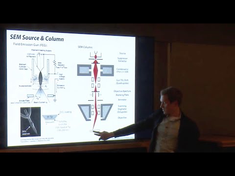
get higher resolution note that when you do this your if your sample is magnetic you've magnifier you've magnetized the pole piece and you would get attractive your sample might get attracted up to it so you don't want to do this with magnetic samples okay so now we've shown the analogies across different types of microscopes we'll get into the particulars of SEM here so this is the SEM field emission gun this is the source so what we have is iron ore excuse me a tungsten filament that's our our cathode so we hold that at negative potential
and then we have our anode plate which we hold at ground potential and so say we want a thirty kilovolts Eller ating voltage then we we keep this at negative thirty this at zero and we're able to accelerate our electrons down the column now the way that works that with a field emission gun is that we do run current through that filament so we get some thermionic emission its tungsten and it's hot so we get thermionic electrons but we also apply this electric field so that we are able to lower the work function at the
tip and get more electrons to emit from that tip we even coat the tip with Zarko neum oxide that further lowers the work function and allows us to get more electron emission and a higher brightness of our beam and that's what you're looking for in these systems and what you see here so I mentioned negative potential ground we hold this grid cap at slightly more negative potential so we get our first crossover of the beam here most of those electrons might get collected at the anode plate the ones that pass through are able to accelerate
down the column at with an energy that's proportional to the accelerating voltage as far as the column we've talked about this source up here now we have a first condenser lens and usually you'll have two of these in your SEM the whole point is to take what's a fairly large spot here and ultimately D magnify it into something much smaller so that virtual source might be on the order of tens of nanometers we need to get it down to the order of single nanometers and so we have to demagnetize and we do that through the
series of lenses so you might have to condenser lenses that help you d magnify the beam so but there what the the condenser is doing is it's crossing the beam over somewhere above the the aperture in the system and then the current that passes through will come down through these octave poles so we have scanning in stigmata octupole x' these are electromagnets and they allow us to scan the beam over our sample so we can get a 2d image and we'll see that the stigmata octive poles also allow you to manipulate the shape of the
beam so you can get a nice circular probe for nice sharp images we can apply a voltage to this blanking plate and we can measure the current through an ammeter and also prevents us from exposing our sample to electrons when we don't want it to be and last thing I didn't mention these gun tilt and shift quadruples are used to sort of steer the beam and I'll show examples of doing that so this slide is just to kind of give an overview of the different parameters that are involved the basic ones you want to keep
in mind are the accelerating voltage the probe current and the probe convergence angle and all of these things can conspire to give you a certain probe diameter which as the operator is what you're ultimately concerned about when you're thinking about the resolution of your images and there's relevant equations that are involved we won't go through them all today on the slides where I go through things like voltage and current I'll keep the relevant equations there so that we're always reminded that we can dig into the equations and do some calculations but these are the the
main ones that are involved and this DP so this is the ultimate probe size it's a function of all these other ones which you can see up here so it's all about calculating the probe size and that's a function of different aberrations and different the parameters like voltage and current and convergence angle as we said all right so probably the most important parameter is the voltage and this is usually what you want to decide upon first when you're looking to optimize your image so the voltage controls the energy of electrons in your system we on
a typical SEM will have as high as 30 kV accelerating voltage and as low as maybe a half a kV or maybe 0.1 kV or even lower and so if we have 30 kV then on average each electron has 30 ke V in energy 15 is 15 ke B 5 is 5 okay and so the higher the energy when the beam makes contact with your sample the the deeper it'll penetrate and scatter and so we refer to this as an interaction volume you might also hear it called an excitation volume and so you can see
that interaction volume gets smaller at lower voltage and this is simulated for silicon there's a scale bar here 1 micron so at 30 kV and silicon looking at about 8 microns deep this is like two and a half at 15 and only a couple hundred nanometers at five now we see that the interaction volume is broken up into different colors and we'll talk about all those different interactions as we proceed now when we want to image we would want the highest voltage should theoretically give us the highest resolution because for one thing high energy if
we look here higher energy gives us a smaller wavelength and therefore we can theoretically form a smaller probe but we're not really wavelength limited in an SEM we're really limited by aberrations in the system and it turns out that spherical aberrations and chromatic aberrations are worse at lower voltage by spherical aberrations I mean the imperfections in the lens so if if you have imperfections in your lens then the farther out your your electrons go the more subject they are to those aberrations and also the longer time they spend in the lens the more subject they
are to aberration so higher voltage that electrons have higher energy they're literally traveling faster through the lens so they're not going to be affected by these aberrations as much chromatic aberrations are the range of energy spread of electrons coming from the tip and will get a smaller energy spread at higher voltage and therefore all of your electrons will be closer to each other in wavelength as they pass through the lens and therefore can get focused down better into a small probe so it's really about aberrations and the aberrations are are not as bad at higher
voltage so we can get higher resolution there now with that's true for conductive specimens so here this is just gold on carbon we have a much sharper image at 30 kV vs. 15 vs 5 but if you have a non conductive specimen that doesn't really help you because putting all this electron negative charge into your sample you can build up charge your beam will start deflecting you're not going to get a nice image you'll get a lot of artifacts but people often call charging artifacts so if we have a non-conductive specimen like this it actually
becomes more useful to image at lower voltage because at lower voltage we have more secondary electron yield and we'll talk about secondary electrons and so our current in versus current out we can actually get to an equilibrium by going to a progressively lower voltage so like here we have just as much current going out as signal as going in and therefore we're not worrying about accumulating charge and we can get artifact artifact free images another thing to think about at 30 kV if the interaction volume is literally larger than the features you're trying to image
then electron secondary electrons will spill out all different surfaces and your sample will end up looking translucent so if you have small features like this like these small beams the low voltage is good if it's non conductive as this is its hydroxyapatite and the interaction volume is now smaller than the features and therefore we're confining our secondary electron emission to only the surface we're not getting it spilling out of other surfaces all right so now we have our SEM current and one way to think about current is that it controls the spot size so everything
controls spot size as I said or the probe size but here we have some some numbers from an old jeol presentation at 22 Pico amps we might get a 2 nano meter probe size that's the best about the best you're gonna do in an SEM and then 400 P clamps maybe 3 nanometers and then it starts to get large or say 10 nanometers or up around a nano amp and of course this isn't we don't have a spot like this there's like a Gaussian profile tis about half of the probe current in in that diameter
and if we look at the images formed with these different currents we'll see that we have sharper features at low current with a smaller probe size and more blurry image when we have a larger probe size here and so what we want to think about when we do when we were changing the current is while we when we lower current will get a smaller probe diameter for a better resolution but will also get less signal so you're really balancing your probe diameter and therefore your resolution versus the amount of signal that you get and I
have a tip here that if you're trying to figure out what current to use look at the contrast value on your system so if your contrast is really high like 95 98 percent then you you can't afford to go to lower current because you won't be able to to maximize the grayscale range of your image if anything you'd want to have more current so that you can you can spread and get better contrast but if you're if your contrast values in the 50s 60s 70s that tells you you have more current than you probably need
or more signal than you need and you can lower the current and therefore it increase the resolution alright so how do we control current we do that through apertures and we do it through the condenser lens or condenser lenses if you have more than one so aperture is pretty simple we can just vary the the physical size of the aperture smaller apertures let through fewer electrons but it's not just that it's that we let through electrons that are more on axis and you want on access electrons because when they enter the objective lens we'd like
them to be closer to the center of the lens so they can come to a point if we have a larger aperture we'll get electrons that are spread over a larger range and it's going to be harder to get them to focus back down to a small probe and that's why you get worse resolution with a higher aperture or a larger aperture all right so here's our aperture wheels we can just physically select them on our microscope sometimes you'll have an automatic aperture changer it's all the same but the the next thing we think about
is the condenser lens so what the condenser does is it's going to change where this crossover point happens inside of the column so if I go here we have a unitless metric called spa so say spot 7 on our microscopes is really high current so we're crossing the beam over basically here I'm at the aperture plane which means we take all of this current and we slide it through the aperture and it's going down to your sample if we increase the strength of our condenser lens then we force these electrons to cross over higher in
the column so now we have a spread beam illuminating our aperture and we'll get fewer electrons through and then if we increase the condenser further then it spreads more and we get fewer electrons so usually you'll have like seven different condenser settings so if you think whatever size your aperture is this might be spot one two three four five six seven so a more condensed beam you'll get more current through a less condensed beam you'll get less and again the angle of those electrons will matter because if you're more condensed then you're gonna get all
these through and then as they get down the column they'll have to get brought back together but if you spread it out wide you're only going to get these on access electrons through your aperture and here we see some of those relationships that I was talking about in terms of condenser lens strength to probe diameter resolution and signal okay so so this is an interaction volume and we're gonna build it out and learn about all the different signals that are involved so the first signal and the primary signal that most people think about and care
about is the secondary electron signal so if we have a primary electron from the beam it's going to inter interact any elastically with the electrons in your atom those electrons will get kicked out and we call them secondary electrons so they're low-energy usually 50 electron volts and it's not and I have it colored here blue at the surface this is where they're coming from the truth is we generate them everywhere but the only ones with enough energy to escape are in this top part of the interaction volume so they're able to only the top 5
10 nanometers can we get a mission and therefore when we collect our image we're taking signal from the top 5 10 nanometers therefore we're gonna see the topography of the image and so we have something like an ever heart Thornley detector where we put a positive bias on it we attract the electrons to it and that's how we end up counting the electrons at each pixel more electrons at a pixel is a brighter pixel fewer electrons is a darker pixel if we put say a thousand by a thousand of those together we get a nice
2d image we also have usually a detector inside the column on these fei systems we call it a through the lens detector other systems call it something different but we can put a positive bias on that and we can attract secondary electrons up into the column and detect them that way this is has will have directional shadowing and this will have sort of radially symmetric shadowing and then we'll see this is also used to do the highest resolution imaging on our systems next we can talk about backscattered electrons and so those are electrons that are
elastically scattered by the atoms in your specimen and so because they're elastic ly scattered they lose less energy so they usually emerge with say fifty to a hundred percent of their original energy so you had thirty ke V electrons from a 30 kV beam there go to emerge with something like 15 to 30 kV which means they can emerge from deeper in the specimen so they're not going to be very good at showing you the surface topography because they're not literally coming from the surface but rather they're going to show you atomic number contrast because
the elastic scattering is a function of the atomic number so a Gold atom will elastically scattered more electrons than say a silicon and therefore your gold will appear brighter on the screen if you have a backscattered electron detector there to collect that signal now one thing I do want to point out so this is a really nice Zee contrast image of gold and titanium and silver on silicon and they're all bright according to their order of Z we also can kind of see some pretty good Zee contrast here with gold on silicon so it is
a little bit easier to to emit or a secondary electron from a higher Z element like gold than it is from silicon so you do have some atomic number contrasts just through secondary electrons but if you want to pure a pure Zee contrast image you want to use a backscattered electron detector and then lastly here we generate characteristic x-rays so if we have a primary electron knock out an inner shell electron an outer shell electron will drop from high to low energy and when it does so it will emit a photon of equivalent energy and
that photon is on the order of an x-ray and so every element has its own energy transitions and therefore emits its own characteristic x-rays and you actually emit them from the whole volume but the characteristic ones usually come from this spike shape and that's something that we can see when we do Monte Carlo simulations of beam specimen interactions and I show that in a different video on YouTube I go through how you can simulate the interaction volumes for your materials and show exactly why I draw it like a spike in that way but the x-rays
that are in line of sight to the x-ray detector are the ones that get counted and they get used to generate a spectrum that will show you which elements are in yours and here we do mapping so we've taken that and we've broken it up into its silicon gold silver and titanium maps and we can see exactly where they all come from all right and so on your handout I also have a table like I have here and it gives you some guidelines on which detectors you're going to use what information you're going to detect
with them and about what the recommended current range that you will need so we generate a lot of secondary electrons so we don't need a lot of current to to get a good signal to noise image which is good because you can operate at low current which means high resolution for your topographic image you need more current for backscattered electrons because the elastic events are more rare so you need to really increase your current to get enough signal and then she won't have a good resolution in that and then you need much more current usually
for x-rays because while we do generate a lot of them only these on this small solid angle this line-of-sight to the detector those the only ones that we count so you do need to be in the nano amp range typically all right so just showing these in larger magnification here you can see a secondary electron image you see all the topography all these imperfections when we go to the back scatter image the image flattens out a little bit you can still see some of this but it's it's much flatter I would say but better Z
contrast and in our our EDS maps we we can see the elemental contrast okay now one thing I in those little data bars I had different voltages used for the different collecting different signals and I'm going to show why you might choose a different voltage to capture these different signals so we have our our interaction volume here for 30 kV and this is what it looks like in the simulation software this is casino Monte Carlo software you can download that it's free and you can use it so that's what it will look like when you
just run the simulation these blue paths are reabsorbed electrons and the red paths are backscattered electrons so that's kind of how I'm drawing this the the overall shape of the image and where I'm getting the backscattered volume we can also look at the energy by position map and we can see that the electrons have the most energy where they enter here sort of like a hot spot and then as the electrons scatter they lose energy and therefore can't create as many characteristic x rays so when you're forming your your spike for your x rays if
you're going to get most of them up here and it's going to trail off as it goes deeper in the specimen okay so when I did those images I did chose 30 kV so the highest voltage a low current 50 Pico amps and a small working distance and I'll talk about working distance but that's going to give me the best resolution for this topographic image and even though the interaction volume is really large the only ones that we actually use for the image like I told you are the ones from the top five ten nanometers
so it doesn't matter about dumping all that charge into our sample as long as it's conductive for the backscattered electron image these are metal films and they're only about I think 20 30 nanometers thick and so if I want to have gold on titanium here if I want this to look like gold and not like the titanium that's beneath it I need to keep the backscattered volume confined to the the top layer of gold so at 30 kV or excuse me 3 kV the entire interaction volume is in the titanium and especially the backscatter volume
is in titanium so you don't see any contribution to the gold from the titanium below it and so that's three kV it's a higher current about an order of magnitude higher 500 Pico amps and I use a different working distance and again I'll talk more about that here for x-rays we need to know where that spike is going to be or where the hot spot will be so it's going to be about here but we so you see some of this electrons scattering through we need to have a high enough energy so that we can
excite x-rays from all the different elements so the highest energy was silver 2.96 ke V so you typically want your voltage to be about two times higher than your highest x-ray that you want to to capture so probably should have went to 6 kV but I think I was keeping it at 5 to try to confine that interaction volume as close to the surface as possible but the general rule of thumb as I say down here 2 times the voltage of the highest energy that you're trying to detect okay and so here's a slide on
energy and wavelength dispersive spectroscopy so in EDS you're just getting all of your different x-rays all the different energies to the detector all at once so you can form a spectrum at like get you get all your elements at one time and then in wavelength dispersive spectroscopy we have an analytical crystal or usually several of these and what we do is we sweep an energy range so we can change the crystal we can change its angle and what we ultimately do is if we're trying to filter out and say how many counts or how many
x-rays we have at a certain energy only those x-rays that satisfy the Bragg condition and diffract and hit the detector will get counted so we slowly cycle through all the energy and therefore we're able to get ultimately what is a higher resolution spectrum so here the outline is eds it's going to be a broader spectrum and the WDS will be much sharper so you can get better modification with WDS but it's a slower technique alright so now we can talk about working distance this is literally the distance from the objective lens to wherever the focal
plane is and so as we change the strength of that lens by changing how much current we flow through that current loop we're changing the negative magnetic field and therefore changing where this beam crosses over as a crossover point or a focal point so practically what we usually do is we get the image in focus a sharp image means we're scanning a small probe over the sample and then we tell the microscope we hey this is where our sample is so if this is telling me I'm eight millimeters away we click a button and that
becomes the coordinate system for the microscope it knows now your sample is eight millimeters away and it can navigate according to that so that's the practical side and if you then change focus your Z on your microscope will stay the same it knows your sample is still there but you're just moving your focal plane up and down the theoretical side is that the convergence angle of the beam will change with the working distance so if we have a short working distance we have a steep convergence angle and the equations would show us that we're going
to get a smaller probe size and if we have a longer working distance we have a more parallel beam of a shallow convergence angle and we're gonna get a poor resolution from the larger spot size if we look at these two images the other side of working distance is the depth of field so we have an inverse relationship between the resolution and the depth of field so if we have this long working distance we don't have great resolution but we'll have really great depth of field so these are two pretty large trusses from the greer
group here and there they're tilted and there are a couple hundred microns apart but we're seeing them both in focus at the same time I put the focal plane somewhere in between them and I can see them both with similar resolution whereas at Short working distance if I do the same thing so this is 6 millimeters versus 24 then I can only get this one in focus and the one in the ak falls out of focus so think of your working distance as a balance between depth of field and resolution we also can change well
here's the resolution so a shorter working distance we have sharper features here and at longer working distance we have a little more wiggles and the beam so we have a poor resolution the spot size or the probe size is also larger but as this tip says practically speaking you're probably going to be confined geometrically by something else if you're doing gallium focused ion beam we'll see that you're gonna be at what's called u centric height and if you're doing EDS you're gonna be at the optimum height where you get the most x-rays to the detector
so this is really this balance of resolution depth of field is really when you are just trying to do imaging only I mentioned you centric height that is a height in the chamber where at any tilt angle will be imaging the same thing and we'll see it's very important for us to be able to image what we cut at the same time at any different angle so here I tilt to 52 degrees and that to zero and we see that this corner that I'm looking at is in the same spot so you always most of
the time you want to do your work at U centric height it's a good way to have a geometrically reproducible spot in your chamber so from week to week to week your samples always in the same place and you can compare all of your images exactly to one another and then we'll talk more about this as it relates to using gallium focused ion beam in the next lecture alright so I just want to show a couple videos through the next couple minutes so we we can watch this happened hopefully all right so here I'm tilted
to zero degrees and we can see this K and I Caltech logo as we start to increase the tilt angle ideally this wouldn't be moving at all if it didn't move at all we would be at U centric height if it moves a little bit that just means we need to make a slight adjustment to the Z and so once we get there to 45 degrees I'm just doing a little thing where I'm lowering the height of the sit of the sample now it's back to where I started from and now if I tilt back
to 0 degrees it's gonna stay stationary in the middle of the screen so that means I'm at U centric height and your microscope is set to be safe at U centric height so if you're a high tilt you should be safe even if it looks unsafe okay alright so there are different imaging modes so I talked about field free mode where we just have that single objective lens this is what gold nanoparticles might look like at 5 kV and and low current this is what they would look like with the immersion lens where we are
as I said having a smaller effective working distance so here's our objective lens plane that's giving us this image now our objective lens plane is floating and it's closer to the sample so while our our physical working distance didn't change the effective working distance of the beam has changed because we it's smaller here so we can get a steeper convergence angle and get the benefits of higher resolution from that what this does though when we have this this magnetic field here we can't get electrons out to the Eberhardt currently detector but we can funnel them
very efficiently up to the TLD that's inside the column and we're gonna get high signal in addition to the small probe size so that's how we do immersion mode imaging then you also have something called weak immersion or also called EDS or edx mode and the purpose of this is it kind of gives us resolution in between these two but but or what it's there for is to trap these electrons funnel them up so you don't have electrons hitting your EDS detector and registering as as x-rays on the detector that would give you a big
background on your x-ray spectrum we also have something called scanning filters so once we've selected voltage current working distance we might end up having some imaging artifacts like we see here so this is one frame where we put the beam at twenty five point six microseconds at each pixel and we're gonna get some horizontal scanning artifacts whereas if we scan the same frame 256 times at point one microseconds and we we average all those frames together we get a nice smooth image and so what's happening is if the beam is dwelling at a long time
at a non-conductive material it builds up a little charge the beam deflects we get some artifacts associated with that whereas if we scan really fast there's not enough time to build up charge on any one frame so every frame is artifact free but it's low signal so we have to average a bunch of these frames together and that's how we get the high signal and no artifacts in our image so we have frame integration frame averaging they're kind of same they're just slightly different averaging is like a moving average integration will just do the total
number that you asked for and then with our some systems a lot of SEMS now have line averaging where you average the same line a bunch of times before going to the next we have that on our helium microscope and I'll talk about that in the helium lecture this is a video that demonstrates this so there's no artifact here but if I have a longer dwell time so it's a longer frame time because each pixel is dwelling longer we get these sort of horizontal artifacts something you can do to test if the artifact is geometric
or if it's real it's like a real something on your system you can rotate the image so just rotate the axis of the scanning axis of the beam and sometimes you won't get as much many artifacts when you say have these squares that are rotated so so that told me I this is an artifact and now I can try to fix it by doing frame averaging so I'm taking a 50 nanosecond dwell time averaging it say 256 times and getting nearly artifact free image okay now on the other side of your handout we have alignments
so we're not going to go through well we'll do a couple small things here on alignments but the basic workflow is you always want to adjust the source tilt so get the beam concentric down the column and then we'll use our focus to tell us if we have in a stigmatism problem and to tell us if we have what's called a lens alignment problem and then we'll fix those things according to what I like to call the visual cues in your image so why would we have something like a stigmatism which will give you stretched
features in your image well if you have astigmatism meaning your beam isn't quite circular its elliptical then it'll be elliptical above the focal plane and then elliptical below the focal plane rotated 90 degrees which always will have a circular beam profile or cross-section at the focal plane and then what you're going to do is use these these stigmata these electromagnets to to try to reshape your beam into being circular so here's a video that demonstrates what happens where if I focus to the right then I get this stretching so I've I've taken that ellipse that's
below the focal plane and I've contacted it with the surface and so here it's I'm getting all these features stretching oh here let me back up a little bit sorry so here I've I'm contacting the sample with an ellipse that's say below the focal plane and then if I move the focus to the other side then I'll get that ellipse to rotate 90 degrees and now it's it's gonna everything will be stretched that way so what you want to do is adjust your focus so that you're halfway in between where it's equally blurry on all
sides and then you will adjust this stigmata to actually tighten up the change the the beam from being elliptical to circular and then you get a nice sharp image and so there are videos like this on YouTube where I talk my way through it and you can follow those to learn more how to do the alignments this one is what's called the lens alignment and so if you move your focus and your images shifting that means your beam is not centered on the objective lens and so because your beam is safe it's on if it's
off-center when you change the strength of the lens it'll cause the beam to deflect so what we do is we will the image which just means wobbling the focus and then we use one of these deflectors these quadruples in the column to get the image or the beam to be centered on the objective lens and now when we change focus it just goes in and out of focus and looks like it blinks in place so those are the two main adjustments you'll make astigmatism and objective lens alignment and so again all these are you can
find on YouTube and you can watch them there now there's another thing that another control we have the detector bias so we have our Everhart throwing the detector and our through the lens detector if we put a positive bias on the Eberhardt throwing the detector will bring in our secondary electrons maybe a couple back scatter electrons will get through but it's mostly secondary electrons we can put a positive bias on the TLD we'll get those secondary electrons will also get some backscattered electrons but it's going to be primarily a topographic image we can also put
a negative bias on the TLD which suppresses our secondary electrons and only lets through backscattered electrons and that will give you more of a Z contrast image we can put a stronger positive bias on the TLD and and bring up a lot of secondary electrons but for some samples like if you have an insulating sample and you're at low voltage that can actually take too much signal off of your sample and it can leave it locally positive which will then give you some imaging artefacts and so what we can do in that case is have
a zero volt bias on the TLD and allow some electrons to go up and some to go back down to the sample and we can get charge equilibrium in that manner so here's a video that shows how we can adjust the the voltage on what we call the suction tube of the TLD so I go to backscattered electron mode it's a negative 50 volt bias you see I lost a lot of my signal because I'm suppressing a lot of it but I put the signal that I get through is going to be show me a
flatter z contrast image if I go back to secondary electrons I get my signal back and it's more 3d or topographic okay so you can see how much more three-dimensional that looks and then if we go to say a custom mode I can actually slide that suction tube voltage and when I go to a higher bias will get more signal so you can use that to increase your signal and when I go negative we lose it all and we just have to adjust our contrast to get our RZ contrast image back all right so that
kind of wraps up all these conditions or the different parameters and that you have this considerations for optimum SEM imaging part of your handout so I'll go through a couple other things here before showing some other examples and applications so we have a measurement calibration standard in our lab so it's a NIST derivative standard so on there we have lines of different spacing so if you want to really check the measurement of your image you can't really trust that everything is 100% accurate these microscopes are usually dialed into like plus or minus one two percent
in terms of their length calibration so you'd want to whatever image settings you use to image your sample take those exact image settings image the the standard at the right size and then just do a comparison so here for instance I was trying to measure something that was on the order of 10 nanometers these lines and so we looked at 100 nanometer center-to-center distances and just did the easy calculation to figure out that you know I think we were off by just a couple percent but you can then do the adjustment and get the real
measurement value of your features something else we have in the lab sample preparation I mentioned well if your sample is not conductive then you can go to lower voltage and I usually train people to do that because people don't often want to coat their devices with a conductive material because they want to still make measurements on them but if you're able to you can coat your specimen with say carbon we have a carbon evaporator and this puts down like five nanometers of amorphous carbon you won't see it in your image at all even if you're
imaging with at the highest magnification and it's it's really conductive and works really well then we have a oxygen and argon plasma cleaner in the lab so if you ever do SEM and you get these black boxes then what's happening is you're if you have any carbonaceous material on your sample that as the beam hits it your locally heating up that area which evolves off these carbonaceous gases and then because we have secondary electrons flying around we actually can create a plasma locally and we can get chemical vapor deposition of those carbonaceous species back down
onto the surface of your sample and now they're more like localized at the surface and carbon doesn't have a high secondary electron yield so it ends up looking darker so you get carbon coating your sample and then you get these these black boxes so what you could do is put your sample in an oxygen cleaner oxygen plasma remove the carbon and therefore when you go and make your images you won't have these black boxes and you should be able to actually remove this carbon with that oxygen plasma if you want to recover the functionality of
your device after imaging it okay and these are details of that plasma cleaner which we won't go through today all right so here are some notable applications and techniques I mentioned these EBM simulations so a lot of people in our lab especially are doing eb mythography to pattern the different parts of their devices and so when you do that on our electron beam pattern generators they're 100 kilovolt so at 100 kV we know our electrons have 100 ke V and they're actually going to penetrate about 80 microns into silicon where as we talked about with
30 kV and an SEM it's about 8 microns so you have a full order of magnitude difference there but when you're patterning something like a resist layer on the top of your device what matters is not really how deep the electrons go but what's happening at the surface and so if we have even 500 nanometers of poly methyl methacrylate PMMA then we want to know what the resolution will be as we pattern it we want to look at what's happening up there so at 100 kV those electrons are moving faster we can get a smaller
probe size and they're basically slicing through that PMMA in defining a very narrow path through it and that's how you're gonna get good resolution on your resist at 30 kV your electrons already start scattering as they go through that 500 nanometers and that's gonna mean you're gonna pattern a wider spot per per unit pixel that you're exposing now that said you can still do really good lithography at 30 kV we have an SEM that has a pattern generator on it and I've used it to pattern 20 nanometer lines this is titanium liftoff so we did
a we did a patterning SEP deposited titanium lifted off the resist and we're left with a nice arbitrary pattern like this so you can do that you can also do dots and I've done as small as say 17 nanometers again lifting off a very thin metal sample and this requires using a really thin resist layer which you can't always use when you're doing your devices but regardless you can get high-resolution patterning we can also do alignment so I've been using this logo throughout the presentation so this was a three-step process where we went from our
CAD we did titanium liftoff with alignment markers and then we used a backscatter electron detector so now this is all coated with resist so how are you going to see your markers through the resist layer you can't really use topographic signal because it's all they're all buried but you use the backscattered electrons that come through and we get Z contrast between the titanium and the silicon and therefore we can see our markers align to them and then we can write the next step so this was gold K and I Caltech with its own set of
alignment markers and then ultimately we aligned to those and did silver for those dots this is our old logo so you can do these multi-step patterns in device construction in our 30 kV SEM system we also have an environmental SEM in the lab and what's unique about that is we can actually operate at a higher pressure in the chamber using this differential pumping arm to prevent our to prevent gas from traveling up the column in oxidizing the tip and we have a couple of different detectors and what it's really useful for are two things one
imaging biological specimens where we don't want them to dry out at high vacuum so we can maintain their morphology with a higher pressure so something on the order of a single mil bar or 10 we can go from 0.1 227 millibar whereas our vacuum and in the high vacuum system is on the order of e minus 5 e minus 6 millibar so we're about five six orders of magnitude higher and these are this is a artificial plasma membrane and we're seeing even down to surface texture on the order of of single nanometers the other thing
we can use it for is to image really non-conductive specimens so when you the way that you have the high pressures you have water vapor in the chamber and so that water vapor is pretty good at wicking away charge that would otherwise accumulate on your specimen so if you have a highly non conductive specimen you put it in at high pressure with the water vapor and you can image it with without coating it with anything so this was done I think with all the tricks that I could pull on the one of our immersion mode
systems and this was done with fairly little effort on the environmental SEM so you get a little bit different contrast but ultimately we're imaging the same kinds of features on this three five material on glass we have an electrical probe station in the lab so it's a 4 point probe station it fits over the stage we're able to guide the probes to our different contact pads and do various measurements depending on what kind of function generator that you hook up to the system we have a hot in the cold stage so we can both heat
up the stage I think to 240 C and we can use liquid nitrogen to run nitrogen gas through it like a heat exchanger cools down the gas that gas flows through the stage and it can cool it down to negative 185 C so you can use this as a way to image your specimen at higher low temperature alright some other techniques and then we're about to wrap up so one thing I don't have a full presentation on atomic force microscopy AFM but it's a really good technique to use to to confirm what you're seeing with
an SEM so an SEM we talked about it gives you topographic contrast things look 3d in nature but it doesn't tell you quantitatively how 3d in nature you can tilt your sample and you can actually make a measurement in cross-section and you can you can be pretty confident with that but if you're just looking at say like the profile of your nanoparticles or something you're not going to be able to extract quantitative topography data from it so an AFM is a stylus and we usually operate it in an in a tapping mode and you kind
of tap it physically along your sample and it's able to very accurately measure the Z topography so this is a great way like I said to to confirm what you're seeing with SEM there's lots of different modes it's not just topography you can measure things like the magnetic field as a function of 2d space electric field you can do surface potential you can do piezo electric kind of measurements so there's all sorts of types of scanning probe measurements you could do our particular AFM has something called peak force tapping mode and it allows you to
generate a force curve for every tap so we we oscillate at two kilohertz so we can generate two thousand force curves first per second or a force curve for every pixel that you're scanning and then by going in and looking at the shapes of these curves and the different components of it you can end up extracting mechanical property data from it so you can even figure out sort of qualitatively quantitative information about the elastic modulus for instance or the adhesion forces that are there it does take some calibration in order to really call it quantitative
but that is something that is available in our lab I also don't have a full presentation on transmission electron microscopy our tems but we do have two tems in our lab a 200 kV system so if we want really high resolution we talked about going higher and voltage to get higher energy electrons smaller wavelength so now we can give 200 ke V and on this one we can have 300 ke V and so we're gonna go progressively higher in resolution and be able to do atomic scale imaging so all the different parameters are here you
can look up the presentation at home and we have like I said on the wiki you can go and look up all the different materials we have for these tems some examples here are imaging quantum dots and what's called high resolution TEM mode where you can see lattice planes of these quantum dots we did some bright field imaging of metal insulator metal insulator middle devices and this was a grain boundary study to kind of see when we do an evaporation of I believe that was aluminum what kind of twin boundaries do we have what kind
of grain boundaries do we have what is the the grain size that we have this is not information that's readily available in an SEM especially this is like you know 50 60 nano meters about the thinnest we can do in an SEM in cross-section we've we've seen 10 nanometers but you're not going to really get that kind of contrast with you know grain boundaries and twin boundaries this is a quantum cascade laser so molecular molecular beam epitaxy of all these different layers as small as one nanometer so here we're seeing in cross-section what that quantum
cascade layer looks like in the TEM and then of course you could do diffraction studies in a TEM where you analyze the the crystallinity of your sample what crystal planes you have what the spacing is of your lattice and that's all done through electron diffraction and what I'll go through in the next lecture on gallium fib and a little bit later on helium fib is how we can make these samples so we we want to extract a very thin sample that's how you do tea and you need a very thin sample usually 100 nanometers or
thinner and we can use the gallium focused ion beam to physically cut it free and extract it from the sample so in the next lecture I'll talk about how we can use a balmy pro but tungsten needle to take a thin sample out of our bulk material that we've cut away with the gallium and how we can weld it to the grid with platinum again using the gallium beam so that we can fin it down to electron transparency in a TEM so get it less than 100 nanometers and then in that lecture I'll go through
all these different examples of gallium fib how we can make we can deposit material make devices this is a silly one but you can make real functional devices by patterning directly with gallium will do cross section I'll show examples of cross sections here is a seven nanometer layer that we were able to image in cross-section this is what a gas injection needle looks like that dispenses the the gas the precursor gas that you use to make a deposition and we'll do some other things like how do you automate your microscope in order to to cut
patterns say say overnight and then the third lecture I'll go through examples of how we we do with the helium and neon focused ion beam so we can get really excellent imaging I'll talk about why we can get better imaging with a helium beam than an electron beam how we can image non conductive materials by balancing the positive charge of helium with an electron flood gun we can do cross sections because we have a gallium fib attached to our helium indium neon system and then I'll show how you can pattern things like graphene nano ribbons
get high aspect ratio patterns and do other kinds of device fabrication at smaller scales than are available with a gallium fiber sometimes even with EB mythography okay so that takes me to the end you have your handouts I showed them at the beginning you have your SEM and out you have your fib handout that will be for the next lecture and we have the alignments handout and I believe that's it so with that we'll end the lecture here and I'll take any questions that you have questions so I know I just hit you out with
a hammer for like an hour and truthfully like design this presentation so that when people ask me questions I send them the like a couple slides you know like in the slides when you download them they have slide notes attached to them so if you had a question about environmental SEM I'd send you the three slides on that and you can read about it but this is just meant to be a resource for you all to to download and use depending on what type of microscopy you're using but it's I think important to understand these
physical concepts that are involved and that's why we spend a lot of time going through this because if you can understand what's going on on this one piece of paper then that's about 95 percent of of the game in terms of being able to optimize your microscopy to get the best results in an SEM alright so if there are questions you guys can stick around and ask maybe we'll we'll use this as an opportunity to end the video recording and we'll see you next week if you want to return for gallium
Related Videos

1:01:08
Gallium Focused Ion Beam (Ga-FIB) Lecture:...
The Kavli Nanoscience Institute at Caltech
16,733 views
16:31
Scanning Electron Microscopy (SEM) Concepts
The Kavli Nanoscience Institute at Caltech
27,987 views

19:54
How do Electron Microscopes Work? 🔬🛠🔬 T...
Branch Education
3,074,673 views
58:49
Introduction to Scanning Electron Microscopy
Ben Britton
6,121 views

23:34
Why Democracy Is Mathematically Impossible
Veritasium
2,998,046 views

21:33
The Difficult Birth of the Scanning Electr...
Asianometry
88,957 views
59:39
An Introduction to Scanning Electron Micro...
NanoBio Node
77,755 views
1:04:13
Helium & Neon Focused Ion Beam (He/Ne-FIB)...
The Kavli Nanoscience Institute at Caltech
3,153 views
23:40
50,000,000x Magnification
AlphaPhoenix
5,522,900 views

20:23
Electromagnetic Waves - with Sir Lawrence ...
Ri Archives
454,775 views

31:14
SEM Theory Course: Session 4 "How do I get...
Microscopy Australia
6,748 views

1:25:34
Investigating the Periodic Table with Expe...
The Royal Institution
1,164,454 views
19:00
Part 1: Electron Guns - G. Jensen
caltech
77,441 views

12:36
Electron beam control in a scanning electr...
Applied Science
81,867 views
55:39
CCEM Webinar Series: Introduction to Heliu...
Canadian Centre for Electron Microscopy CCEM
652 views
46:56
Eva Nogales (UC Berkeley): Introduction to...
Science Communication Lab
146,248 views
46:10
FEI Tecnai F20 S/TEM: high-resolution imaging
Nicholas Rudawski
18,379 views
1:05:28
Introduction to Transmission Electron Micr...
MRL Facilities
15,555 views

16:07
Introduction to the Scanning Electron Micr...
Duke University - SMIF
98,548 views
15:26
I did the double slit experiment at home
Looking Glass Universe
1,958,011 views