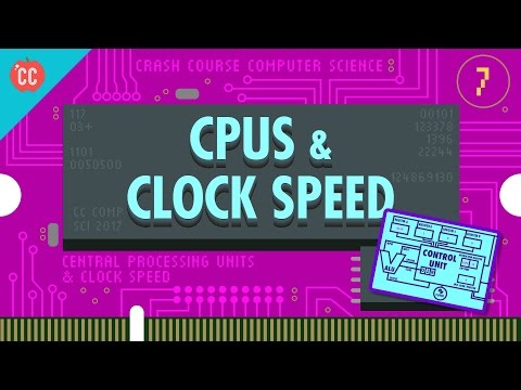
The Central Processing Unit (CPU): Crash Course Computer Science #7
1.63M views2115 WordsCopy TextShare

CrashCourse
Today we’re going to build the ticking heart of every computer - the Central Processing Unit or CPU....
Video Transcript:
Hi, I’m Carrie Anne, this is Crash Course Computer Science, and today, we’re talking about processors. Just a warning though - this is probably the most complicated episode in the series. So once you get this, you’re golden.
We’ve already made a Arithmetic and Logic Unit, which takes in binary numbers and performs calculations, and we’ve made two types of computer memory: Registers -- small, linear chunks of memory, useful for storing a single value -- and then we scaled up, and made some RAM, a larger bank of memory that can store a lot of numbers located at different addresses. Now it’s time to put it all together and build ourselves the heart of any computer, but without any of the emotional baggage that comes with human hearts. For computers, this is the Central Processing Unit, most commonly called the CPU.
INTRO A CPU’s job is to execute programs. Programs, like Microsoft Office, Safari, or your beloved copy of Half Life: 2, are made up of a series of individual operations, called instructions, because they “instruct” the computer what to do. If these are mathematical instructions, like add or subtract, the CPU will configure its ALU to do the mathematical operation.
Or it might be a memory instruction, in which case the CPU will talk with memory to read and write values. There are a lot of parts in a CPU, so we’re going to lay it out piece by piece, building up as we go. We’ll focus on functional blocks, rather than showing every single wire.
When we do connect two components with a line, this is an abstraction for all of the necessary wires. This high level view is called the microarchitecture. OK, first, we’re going to need some memory.
Lets drop in the RAM module we created last episode. To keep things simple, we’ll assume it only has 16 memory locations, each containing 8 bits. Let’s also give our processor four, 8-bit memory registers, labeled A, B, C and D which will be used to temporarily store and manipulate values.
We already know that data can be stored in memory as binary values and programs can be stored in memory too. We can assign an ID to each instruction supported by our CPU. In our hypothetical example, we use the first four bits to store the “operation code”, or opcode for short.
The final four bits specify where the data for that operation should come from - this could be registers or an address in memory. We also need two more registers to complete our CPU. First, we need a register to keep track of where we are in a program.
For this, we use an instruction address register, which as the name suggests, stores the memory address of the current instruction. And then we need the other register to store the current instruction, which we’ll call the instruction register. When we first boot up our computer, all of our registers start at 0.
As an example, we’ve initialized our RAM with a simple computer program that we’ll to through today. The first phase of a CPU’s operation is called the fetch phase. This is where we retrieve our first instruction.
First, we wire our Instruction Address Register to our RAM module. The register’s value is 0, so the RAM returns whatever value is stored in address 0. In this case, 0010 1110.
Then this value is copied into our instruction register. Now that we’ve fetched an instruction from memory, we need to figure out what that instruction is so we can execute it. That is run it.
Not kill it. This is called the decode phase. In this case the opcode, which is the first four bits, is: 0010.
This opcode corresponds to the “LOAD A” instruction, which loads a value from RAM into Register A. The RAM address is the last four bits of our instruction which are 1110, or 14 in decimal. Next, instructions are decoded and interpreted by a Control Unit.
Like everything else we’ve built, it too is made out of logic gates. For example, to recognize a LOAD A instruction, we need a circuit that checks if the opcode matches 0010 which we can do with a handful of logic gates. Now that we know what instruction we’re dealing with, we can go ahead and perform that instruction which is the beginning of the execute phase!
Using the output of our LOAD_A checking circuit, we can turn on the RAM’s read enable line and send in address 14. The RAM retrieves the value at that address, which is 00000011, or 3 in decimal. Now, because this is a LOAD_A instruction, we want that value to only be saved into Register A and not any of the other registers.
So if we connect the RAM’s data wires to our four data registers, we can use our LOAD_A check circuit to enable the write enable only for Register A. And there you have it -- we’ve successfully loaded the value at RAM address 14 into Register A. We’ve completed the instruction, so we can turn all of our wires off, and we’’re ready to fetch the next instruction in memory.
To do this, we increment the Instruction Address Register by 1 which completes the execute phase. LOAD_A is just one of several possible instructions that our CPU can execute. Different instructions are decoded by different logic circuits, which configure the CPU’s components to perform that action.
Looking at all those individual decode circuits is too much detail, so since we looked at one example, we’re going to go head and package them all up as a single Control Unit to keep things simple. That’s right a new level of abstraction. The Control Unit is comparable to the conductor of an orchestra, directing all of the different parts of the CPU.
Having completed one full fetch/decode/execute cycle, we’re ready to start all over again, beginning with the fetch phase. The Instruction Address Register now has the value 1 in it, so the RAM gives us the value stored at address 1, which is 0001 1111. On to the decode phase!
0001 is the “LOAD B” instruction, which moves a value from RAM into Register B. The memory location this time is 1111, which is 15 in decimal. Now to the execute phase!
The Control Unit configures the RAM to read address 15 and configures Register B to receive the data. Bingo, we just saved the value 00001110, or the number 14 in decimal, into Register B. Last thing to do is increment our instruction address register by 1, and we’re done with another cycle.
Our next instruction is a bit different. Let’s fetch it. 1000 01 00.
That opcode 1000 is an ADD instruction. Instead of an 4-bit RAM address, this instruction uses two sets of 2 bits. Remember that 2 bits can encode 4 values, so 2 bits is enough to select any one of our 4 registers.
The first set of 2 bits is 01, which in this case corresponds to Register B, and 00, which is Register A. So “1000 01 00” is the instruction for adding the value in Register B into the value in register A. So to execute this instruction, we need to integrate the ALU we made in Episode 5 into our CPU.
The Control Unit is responsible for selecting the right registers to pass in as inputs, and configuring the ALU to perform the right operation. For this ADD instruction, the Control Unit enables Register B and feeds its value into the first input of the ALU. It also enables Register A and feeds it into the second ALU input.
As we already discussed, the ALU itself can perform several different operations, so the Control Unit must configure it to perform an ADD operation by passing in the ADD opcode. Finally, the output should be saved into Register A. But it can’t be written directly because the new value would ripple back into the ALU and then keep adding to itself.
So the Control Unit uses an internal register to temporarily save the output, turn off the ALU, and then write the value into the proper destination register. In this case, our inputs were 3 and 14, and so the sum is 17, or 00010001 in binary, which is now sitting in Register A. As before, the last thing to do is increment our instruction address by 1, and another cycle is complete.
Okay, so let’s fetch one last instruction: 01001101. When we decode it we see that 0100 is a STORE_A instruction, with a RAM address of 13. As usual, we pass the address to the RAM module, but instead of read-enabling the memory, we write-enable it.
At the same time, we read-enable Register A. This allows us to use the data line to pass in the value stored in register A. Congrats, we just ran our first computer program!
It loaded two values from memory, added them together, and then saved that sum back into memory. Of course, by me talking you through the individual steps, I was manually transitioning the CPU through its fetch, decode and execute phases. But there isn’t a mini Carrie Anne inside of every computer.
So the responsibility of keeping the CPU ticking along falls to a component called the clock. As it’s name suggests, the clock triggers an electrical signal at a precise and regular interval. Its signal is used by the Control Unit to advance the internal operation of the CPU, keeping everything in lock-step - like the dude on a Roman galley drumming rhythmically at the front, keeping all the rowers synchronized.
. . or a metronome.
Of course you can’t go too fast, because even electricity takes some time to travel down wires and for the signal to settle. The speed at which a CPU can carry out each step of the fetch-decode-execute cycle is called its Clock Speed. This speed is measured in Hertz - a unit of frequency.
One Hertz means one cycle per second. Given that it took me about 6 minutes to talk you through 4 instructions -- LOAD, LOAD, ADD and STORE -- that means I have an effective clock speed of roughly . 03 Hertz.
Admittedly, I’m not a great computer but even someone handy with math might only be able to do one calculation in their head every second or 1 Hertz. The very first, single-chip CPU was the Intel 4004, a 4-bit CPU released in 1971. It’s microarchitecture is actually pretty similar to our example CPU.
Despite being the first processor of its kind, it had a mind-blowing clock speed of 740 Kilohertz -- that’s 740 thousand cycles per second. You might think that’s fast, but it’s nothing compared to the processors that we use today. One megahertz is one million clock cycles per second, and the computer or even phone that you are watching this video on right now is no doubt a few gigahertz -- that's BILLIONs of CPU cycles every… single.
. . second.
Also, you may have heard of people overclocking their computers. This is when you modify the clock to speed up the tempo of the CPU -- like when the drummer speeds up when the Roman Galley needs to ram another ship. Chip makers often design CPUs with enough tolerance to handle a little bit of overclocking, but too much can either overheat the CPU, or produce gobbledygook as the signals fall behind the clock.
And although you don’t hear very much about underclocking, it’s actually super useful. Sometimes it’s not necessary to run the processor at full speed. .
. maybe the user has stepped away, or just not running a particularly demanding program. By slowing the CPU down, you can save a lot of power, which is important for computers that run on batteries, like laptops and smartphones.
To meet these needs, many modern processors can increase or decrease their clock speed based on demand, which is called dynamic frequency scaling. So, with the addition of a clock, our CPU is complete. We can now put a box around it, and make it its own component.
Yup. A new level of abstraction! RAM, as I showed you last episode, lies outside the CPU as its own component, and they communicate with each other using address, data and enable wires.
Although the CPU we designed today is a simplified example, many of the basic mechanics we discussed are still found in modern processors. Next episode, we’re going to beef up our CPU, extending it with more instructions as we take our first baby steps into software. I’ll see you next week.
Related Videos

10:36
Instructions & Programs: Crash Course Comp...
CrashCourse
960,752 views

35:33
How does Computer Memory Work? 💻🛠
Branch Education
4,131,807 views

11:10
How Computers Calculate - the ALU: Crash C...
CrashCourse
2,003,583 views

10:40
How Do CPUs Work?
ExplainingComputers
288,360 views

12:17
Registers and RAM: Crash Course Computer S...
CrashCourse
2,143,013 views

13:08
We Fell For The Oldest Lie On The Internet
Kurzgesagt – In a Nutshell
2,960,114 views

9:04
The Fetch-Execute Cycle: What's Your Compu...
Tom Scott
1,868,186 views

20:42
How a CPU Works
In One Lesson
8,309,635 views

15:42
RAM Explained - Random Access Memory
PowerCert Animated Videos
3,096,550 views

18:11
How Amateurs created the world’s most popu...
LowSpecGamer
913,361 views

13:36
Operating Systems: Crash Course Computer S...
CrashCourse
1,594,725 views

7:55
Fetch Decode Execute Cycle in more detail
Computer Science Lessons
558,285 views

12:23
Advanced CPU Designs: Crash Course Compute...
CrashCourse
932,074 views

1:17:35
4. Assembly Language & Computer Architecture
MIT OpenCourseWare
722,329 views

14:24
Explaining RISC-V: An x86 & ARM Alternative
ExplainingComputers
463,107 views

24:56
How do Smartphone CPUs Work? || Inside t...
Branch Education
1,992,397 views

13:50
Integrated Circuits & Moore's Law: Crash C...
CrashCourse
653,347 views

21:20
Cracking Enigma in 2021 - Computerphile
Computerphile
2,527,149 views

14:28
HOW TRANSISTORS RUN CODE?
Core Dumped
515,773 views