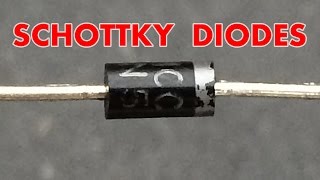
What is a Schottky Diode? How Schottky Diodes Work? Where to Use? ( Schottky Diode Tutorial)
825.44k views1423 WordsCopy TextShare

Electrical Electronics Applications
In this video, I will explain to in detail the structure, working principle and places of use of Sch...
Video Transcript:
Hi guys! In this lesson, I will explain to in detail the structure, working principle and places of use of Schottky diode, which we can encounter in communication circuits, power circuits and many other places. At the end of the video, you will have access to a lot of information about this diode.
Normal diodes cannot respond to the reversal of the applied voltage at very high frequencies. In other words, they cannot change from a conductive state to an insulating state or from an insulating state to a conductive state. Schottky diodes are produced to be used in computers, RF and rectifier applications that need high switching speed in order to respond to these rapid changes.
Like the Silicon diode, which consists of normal doped PN structure, Schottky diode has an anode and a cathode pin. This diode also has a white stripe at the cathode pin. If the current is going from the anode to the cathode, the diode allows the current to flow and prevents it from going in the opposite direction.
Here, a question has definitely come to your mind, what is the difference between this diode and a normal silicon diode. So, let's examine the difference one by one. First of all, let's start with how the symbol of the Schottky diode is.
Its symbol is as you see it here. Here's how you can remember the symbol. Instead of a line at the cathode pin of the diode symbol, there is an S-like but angular shape.
Schottky diodes are not only produced with two pins, but also with three pins as here. In these diodes, the cathode pins of two Schottky diodes are combined. In other words, there are two Schottky diodes inside these three-pin ones.
Looking at the internal structure, these diodes have lower forward voltage drop compared to ordinary silicon PN junction diodes. Normal Silicon diodes consist of combining P-type and N-type doped semiconductors, as here. The junction point, which is the neutral region of the P and N structure, is wide.
Schottky diode, on the other hand, consists of combining the N-type doped semiconductor with a metal-clad P-doped semiconductor. In addition, the junction points in the middle, that is, the neutral zone, is thinned and it is easier for the current to exceed the neutral zone. It consists of a metal/semiconductor combination.
Here, the P-type region usually consists of a metal anode such as gold, silver, platinum, tungsten, molybdenum or chromium. Thus, it can provide conduction at much lower forward voltage levels than normal PN type Silicon diodes. We can compare the two types of diodes as follows.
There is a normal PN-shaped diode made of Silicon on the left, and a Schottky diode formed as a Metal/Semiconductor on the right. A voltage between about 0. 6V and 0.
7V is needed for the normal diode made of silicon on the left to conduct, while a voltage between 0. 2V and 0. 3V is sufficient for the Schottky diode, which is made up of Metal/Semiconductor combination, to conduct.
You may have a question on your mind, friends. You can say what would happen if there was such a small difference. Now we will look at the advantages of this one by one.
Especially in communication systems, operations are carried out with voltages at milli volt levels. Therefore, even such a difference in the systems there is very important. First, let's examine the differences in the power they expend.
For example, let's assume that a current of 10A flows through the silicon diode on the left. A voltage value of 0. 7V is needed for it to transmit.
In other words, 0. 7V will be measured on it when it turns on. If we calculate the power consumed by this diode; It will be a value like 7W from the formula P=VxI.
Let a current of 10A flow through the Schottky diode on the right in the same way. Let's assume that a voltage value of 0. 3V is needed for this to transmit.
The power consumed by this shock diode will be 3W from the formula P=VxI. From these results, we can see that the wasted power value on the Schottky diode is less. If this power value is in a circuit with higher current, it will create much higher differences.
Therefore, the low value of this power, which is wasted on the Schottky diode, will provide an advantage in terms of efficiency. This situation also affects the voltage value falling on the load. For example, a 2V source on the left is connected in series with a load with a Silicon diode.
Since 0. 7V will remain on the diode, 1. 3V can be transferred to the load.
In the circuit on the right, the voltage source with the same value is connected in series with the load with the shock diode. Considering that 0. 3V remains on the shock diode, 1.
7V will remain on the load. This very small difference is often important, especially in communication circuits. We can show the transition thresholds of the diodes over the Current-Voltage graph as follows.
Current-Voltage graph of normal Silicon diode is shown as here. After about 0. 7V voltage, it starts to pass current and becomes forward biased.
We can show the current-voltage graph of the Schottky diode in this way. After about 0. 3V voltage value, it will start to pass current and become forward polarized.
We can also look at the advantage of the Schottky diode over frequency. Here you see a half-wave rectifier circuit. With this circuit, only the positive alternans are transferred to the output by preventing the negative part of the input voltage from passing through, thanks to a single diode.
Here, there is no problem when we make the rectification process over an AC with a frequency of 60Hz used in the city network. But, if the frequency value is much higher than 60Hz, for example, if it has a frequency value such as 5KHz, the diode at the output cannot respond quickly to negative alternans, and as you can see here, unwanted transitions to negative alternans occur. But if we use a Schottky diode instead of a normal diode, this problem is eliminated since the Schottky diode will respond faster at high frequencies.
In this case, it gives us an advantage in high frequency circuits. Here you see a DC-DC Boost Converter. The circuit diagram is basically like this.
The upgrade process is based on the switching speed of the MOSFET in the circuit. In this circuit, triggers are made at high frequency values at the KHz level. Therefore, instead of using normal silicon diodes to respond to high frequency switching speeds, Schottky diodes are preferred in order to obtain healthier results.
Here you see an Amplitude Modulation circuit. Thanks to this modulation, it can be transmitted over much longer distances using lower power transmitters than is possible using VHF or UHF signals. We see that Schottky diodes are used here for the demodulation of small amplitude waves.
There are many communication devices, especially in aviation and space systems, where VHF or UHF signals are used, where AM Modulation is made. An example of one of the places where Schottky diodes are used is RF Mixer circuits. Schottky diodes are used in RF Mixer circuits used to move the frequency of a signal from one band to another band.
When we look at the circuit diagram, we can see that there are four choke diodes in the full wave rectifier structure in this way. Thanks to the RF Mixer, the incoming audio signal is encrypted and sent to another receiver at a different frequency value. In addition, these RF Mixer are used in circuits wherever radio frequency signals are used, from radio receivers to radio transmitters to radar systems.
Another example of usage is solar panels. Two groups of diodes, Bypass and Blocked, are used in the connections of solar panels. Blocking diodes are used to protect the panels against reverse current from the battery.
Normal Silicon diodes are used here. Bypass diodes are used to transfer the generated current directly to the battery. Here too, Schottky diodes are preferred since the forward voltage drop is very small.
Thus, the currents produced in the panels connected in series are transferred directly to the battery without going over the other panels and thus they are charged. The structure, working principle and some usage areas of the Schottky diodes are basically like this. I hope it was helpful and you liked it.
Hope to see you in our next lesson. Goodbye.
Related Videos

5:22
What is a Zener Diode? How Does it Work? W...
Electrical Electronics Applications
197,042 views
6:02
What is a schottky diode?
Afrotechmods
2,219,855 views

8:13
How Does a MOSFET Work?
Explorer
1,354,342 views
9:44
Different types of Reverse Voltage Protect...
Foolish Engineer
41,699 views

40:10
Diodes - A Practical Guide
DroneBot Workshop
32,526 views

7:39
Decoupling Capacitors - And why they are i...
Lalo Solo
350,659 views

21:49
Understanding Schottky diodes (with bench ...
JohnAudioTech
73,300 views

10:16
How an Inductor Works ⚡ What is an Inductor
VirtualBrain [ENG]
836,478 views

13:40
DIODES! All Sorts of Them and How They Wor...
ElectroBOOM
1,567,324 views
16:02
5V Regulator design tutorial - How it work...
The Engineering Mindset
3,586,987 views

7:46
MOSFETs and How to Use Them | AddOhms #11
AddOhms
3,731,160 views

13:03
Basic Electronics for Beginners in 15 Steps
Electrical Electronics Applications
569,240 views
32:34
EEVblog #908 - Zener Diodes
EEVblog
474,798 views

5:44
Learn how to test the Schottky diode with ...
Electronics Repair Basics_ERB
47,559 views

9:38
How To Convert DC to AC | Direct current I...
Prof MAD
1,243,098 views
13:39
Power Inverters Explained - How do they wo...
The Engineering Mindset
3,696,867 views

7:31
Electronic Basics #31: Schottky Diode & Ze...
GreatScott!
529,081 views

11:32
Schottky Diode Part 1 - Band Diagram
Jordan Louis Edmunds
69,927 views
14:48
The Big Misconception About Electricity
Veritasium
23,049,781 views

20:39
Power factor explained | Active Reactive A...
Prof MAD
365,653 views