Why It Was Almost Impossible to Make the Blue LED
24.22M views5224 WordsCopy TextShare
Veritasium
The blue LED was supposed to be impossible—until a young engineer proposed a moonshot idea. Head to ...
Video Transcript:
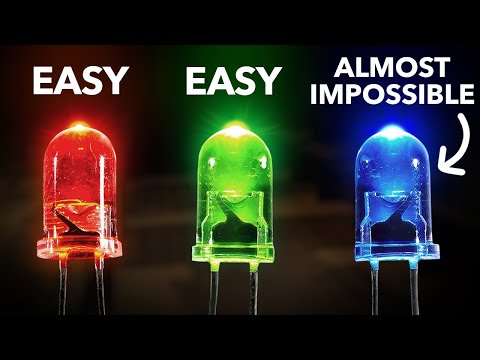
- LEDs don't get their color from their plastic covers. And you can see that because here is a transparent LED that also glows the same red color. The color of the light comes from the electronics themselves.
The casing just helps us tell different LEDs apart. In 1962, general Electric engineer Nick Holonyak created the first visible LED. It glowed a faint red.
A few years after that, engineers at Monsanto created a green LED. But for decades, all we had were those two colors. So LEDs could only be used in things like indicators, calculators, and watches.
If only we could make blue, then we could mix red, green, and blue to make white, and every other color, unlocking LEDs for every type of lighting in the world, from light bulbs, to phones, to computers, to TVs to billboards. But blue was almost impossible to make. (dramatic music) Throughout the 1960s, every big electronics company in the world, from IBM to GE, to Bell Labs, raced to create the blue LED.
They knew it would be worth billions. Despite the efforts of thousands of researchers, nothing worked. 10 years after Holonyak's original LED turned into 20, then 30, and the hope of ever using LEDs for light, faded away.
According to a director at Monsanto, these won't ever replace the kitchen light. They'd only be used in appliances, car dashboards, and stereo sets to see if the stereo was on. This might still be true today, if not for one engineer who defied the entire industry and made three radical breakthroughs to create the world's first blue LED.
(dramatic music) Shūji Nakamura was a researcher at a small Japanese chemical company named Nichia. They had recently expanded into the production of semiconductors to be used in the manufacture of red and green LEDs. But by the late 1980s, the semiconductor division was on its last legs.
They were competing against far more established companies in a crowded market, and they were losing. Tensions started to run high. Younger employees begged Nakamura to create new products, while senior workers called his research a waste of money.
And at Nichia, money was in short supply. Nakamura's lab mainly consisted of machinery he had scavenged and welded together himself. Phosphorus leaks in his lab created so many explosions, that his coworkers had stopped checking in on him.
By 1988, Nakamura's supervisors were so disillusioned with his research that they told him to quit. So it was out of desperation that he brought a radical proposal to the company's founder and president Nobuo Ogawa. (dramatic music) The elusive blue LED, that the likes of of Sony, Toshiba and Panasonic had all failed at.
What if Nichia could be the one to create it? After suffering loss after loss on their semiconductors for more than a decade, Ogawa took a gamble. He devoted 500 million yen or $3 million, likely around 15% of the company's annual profit, to Nakamura's moonshot Project.
Everyone knew that LEDs have the potential to replace light bulbs, because light bulbs, the universal symbol for a bright idea, are actually terrible at making light. They work by running current through a tungsten filament, which gets so hot, it glows. But most of the electromagnetic radiation comes out as infrared, heat.
Only a negligible fraction is visible light. In contrast, LED stands for light emitting diode. It's right there in the name.
LEDs primarily create light, so they're far more efficient, and a diode is just a device with two electrodes, which only allows current to flow in one direction. So here's how an LED works. When you have an isolated atom, each electron in that atom occupies a discreet energy level.
You can think of these energy levels like individual seats from a hockey stadium, and all atoms of the same element, when they are far apart from each other have identical available energy levels. But when you bring multiple atoms together to form a solid, something interesting happens. The outermost electrons now feel the pole, not only of their own nucleus, but of all the other nuclei as well.
And as a result, their energy levels shift. So instead of being identical, they become a series of closely spaced, but separate energy levels. An energy band.
The highest energy band with electrons in it, is known as the valence band, and the next higher energy band is called the conduction band. You can think of it like the balcony level. In conductors, the valence band is only partially filled.
This means with a little bit of thermal energy, electrons can jump into nearby unfilled seats, and if an electric field is applied, they can jump from one unfilled seat to the next and conduct current through the material. In insulators, the valence band is full, and the difference in energy between the valence and conduction bands, the band gap, is large. So when an electric field is applied, no electrons can move.
There are no available seats to move into in the valence band, and the band gap is too big for any electrons to jump into the conduction band, which brings us to semiconductors. Semiconductors are similar to insulators, except the band gap is much smaller. This means at room temperature, a few electrons will have sufficient energy to jump into the conduction band, and now they can easily access nearby empty seats and conduct current.
Not only that, the empty seats they left behind in the valence band can also move. Well, really, it's the nearby electrons jumping into those empty seats. But if you look from afar, it's as though the empty seat or hole is moving like a positive charge in the opposite direction to the electrons in the conduction band.
(soft music) By themselves, pure semiconductors are not that useful. To make them way more functional, you have to add impurity atoms into the lattice. This is known as doping.
For example, in silicon, you can add a small number of phosphorus atoms. Phosphorus is similar to silicon, so it easily fits into the lattice, but it brings with it one extra valence electron. This electron exists in a donor level just beneath the conduction band.
So with a bit of thermal energy, all these electrons can jump into the conduction band and conduct current. Since most of the charges that can move in this type of semiconductor are electrons, which are negative, this sort of semiconductor is called n-type, n for negative, but I should point out that the semiconductor itself is still neutral. It's just that most of the mobile charge carriers are negative.
They're electrons. So there is also another type of semiconductor where most of the mobile charge carriers are positive, and it's called p-type. To make p-type silicon, you add a small number of atoms of, say, boron.
Boron fits into the lattice, but brings with it one fewer valence electron than silicon. So it creates an empty acceptor level just above the valence band. And with a bit of thermal energy, electrons can jump outta the valence band, leaving behind holes.
It is these positive holes which are mostly responsible for carrying current in the p-type semiconductor. Again, the material overall is uncharged, it's just that most of the mobile charge carriers are positive holes. Where things get interesting is when you put a piece of p-type and n-type together.
Without even connecting this to a circuit, some electrons will diffuse from n to p and fall into the holes in the p-type. This makes the p-type a little negatively charged, and the n-type a little positively charged. So there is now an electric field inside an inert piece of material.
Electrons keep diffusing until the electric field becomes so large, it prevents them from crossing over. And now we have established the depletion region, an area depleted of mobile charge carriers. There are no electrons in the conduction band and no holes in the valence band.
If you connect a battery the wrong way to this diode, it simply expands the depletion region until its electric field perfectly opposes that of the battery and no current flows. But if you flip the polarity of the battery, then the depletion region shrinks, the electric field decreases, and electrons can flow from n to p. When an electron falls from the conduction band into a hole in the valence band, that band gap energy can be emitted as a photon.
The energy change of the electron is emitted as light, and this is how a light emitting diode works. The size of the band gap determines the color of the light emitted. In pure silicon, the band gap is only 1.
1 electron volts. So the photon released isn't visible, it's infrared light. These LEDs are actually used in remote controls for your TV, and you can capture them on camera.
Moving up the spectrum, you can see why the first visible light LEDs were red and then green, and why blue was so hard. A photon of blue light requires more energy, and therefore a larger band gap. By the 1980s, after hundreds of millions of dollars had been spent hunting for the right material, every electronics company had come up empty handed.
But researchers had at least figured out the first critical requirement, high quality crystal. No matter what material you used for the blue LED, it required a near perfect crystal structure. Any defects in the crystal lattice, disrupt the flow of electrons.
So instead of emitting their energy as visible light, it is instead dissipated as heat. So the first step in Nakamura's proposal to Ogawa, was to disappear to Florida. He knew an old colleague there whose lab was beginning to use a new crystal making technology called Metal Organic Chemical Vapor Deposition, or MOCVD.
An MOCVD reactor, essentially a giant oven, was and still is the best way to mass produce clean crystal. It works by injecting vapor molecules of your crystal into a hot chamber where they react with a base material called a substrate to form layers. It's important that the substrate lattice matches the crystal lattice being built on top of it to create a stable, smooth crystal.
This is a precise art. The crystal layers often need to be as thin as just a couple of atoms. Nakamura joined the lab for a year to master MOCVD.
But his time there was miserable. He wasn't allowed to use the working MOCVD, so he spent 10 of his 12 months assembling a new system, almost from scratch. Even worse, his lab mates shunned him because Nakamura didn't have a doctorate, nor any academic papers to his name, as Nichia didn't allow publishing.
His lab mates, all PhD researchers, dismissed him as a lowly technician. This experience fueled him. Nakamura wrote, "I feel resentful when people looked down on me.
I developed more fighting spirit. I would not allow myself to be beaten by such people. " (inspirational music) He returned to Japan in 1989 with two things in hand.
One, an order for a brand new MOCVD reactor for Nichia, and two, a fervent desire to get his PhD. At that time in Japan, you could earn a PhD without having to go to university, simply by publishing five papers. Nakamura had always known his chances of inventing the blue LED were low.
But now he had a backup plan. Even if he didn't succeed, he could at least get his PhD. But now the question was with MOCVD under his belt, which material should he research?
By this time, scientists had narrowed the options down to two main candidates, zinc selenide, and gallium nitride. These were both semiconductors with band gaps, theoretically, in the blue light range. Zinc selenide was the far more promising option.
When grown in an MOCVD reactor, it had only a . 3% lattice mismatch with its substrate, gallium arsenide. Therefore, zinc selenide crystal had about a thousand defects per square centimeter, within the upper limit for LED functioning.
Its only issue was that while scientists had figured out multiple different ways to create n-type zinc selenide, no one knew how to create p-type. In contrast, gallium nitride had been abandoned by almost everybody for three reasons. First, it was much harder to make a high quality crystal.
The best substrate for growing gallium nitride was sapphire, but its lattice mismatch was 16%. This resulted in higher defects, over 10 billion per square centimeter. The second problem was that like zinc selenide, scientists had only ever created n-type gallium nitride using silicon.
P-type was elusive. And third, to be commercially viable, a blue LED would have to have a total light output power of at least a thousand microwatts. That's two orders of magnitude more than any prototype had ever achieved.
So between the two candidates, almost all researchers were focused on zinc selenide. Nakamura surveyed the crowded field and decided that if he were going to publish five papers by himself, he'd better focus on gallium nitride, where the competition was much less fierce. This material's main claim to fame was one development back in 1972, when RCA engineer Herbert Maruska made a tiny gallium nitride blue LED, but it was dim and inefficient.
So RCA slashed the project's budget, calling it a dead end. 20 years later, scientific opinion hadn't changed. When Nakamura attended the biggest applied physics conference in Japan, the talks on zinc selenide had over 500 attendees.
The talks on gallium nitride had five. (dramatic music) Two of those five attendees were the world experts on gallium nitride, Dr Isamu Akasaki and his former grad student, Dr Hiroshi Amano. In contrast to Nakamura's academic background, they were researchers at Nagoya University, one of Japan's best.
A few years earlier, they had made a breakthrough on the first problem of high quality crystal. Instead of growing gallium nitride directly on sapphire, they first grew a buffer layer of aluminum nitride. This has a lattice spacing in between that of the other two materials, making it easier to grow a clean gallium nitride crystal on top.
The only issue was that the aluminum caused problems for the MOCVD reactor, making the process hard to scale. But Nakamura wasn't even close at this stage. Back at Nichia, he couldn't get gallium nitride to even grow normally in his new MOCVD reactor.
After six months, desperate for results, he decided to take the machine apart and build a better version himself. His 10 months spent putting together the reactor in Florida, were suddenly invaluable. He began following the same routine each day, arrive at the lab at 7:00 AM.
Spend the first half of the day welding, cutting, and rewiring the reactor. Spend the rest of the day experimenting with the modified reactor to see what it can do. At 7:00 PM go home, eat dinner, wash and sleep.
Nakamura repeated this routine every single day, taking no weekends and no holidays except for New Year's Day, the most important holiday in Japan. (soft music) After a year and a half of continuous work, he came into the lab on a winter day in late 1990. As usual, he tinkered around in the morning grew a gallium nitride sample in the afternoon, and tested it.
But this time, the electron mobility was four times higher than any gallium nitride ever grown directly on sapphire. Nakamura called it the most exciting day of his life. His trick was to add a second nozzle to the MOCVD reactor.
The gallium nitride reactant gases had been rising in the hot chamber, mixing in the air to form a powdery waste. But the second nozzle released a downward stream of inert gas, pinning the first flow to the substrate to form a uniform crystal. For years, scientists had avoided adding a second stream to MOCVD because they thought it would only introduce more turbulence.
But Nakamura used a special nozzle so that even when the streams combined, they remained laminar. He called his invention the two-flow reactor. Now, he was ready to take on Akazaki and Amano, but instead of copying their aluminum nitride buffer layer, his two flow design allowed him to make gallium nitride so smooth and stable, it itself could be used as a buffer layer on the sapphire substrate.
This in turn, yielded an even cleaner crystal of gallium nitride on top, without the issues of aluminum. Nakamura now had the highest quality gallium nitride crystals ever made. But just as he was getting started, things took a wrong turn.
(dramatic music) While he had been in Florida, Nobuo Ogawa had stepped back from Nichia to become chairman. In his day, Nobuo had been a risk taking scientist, designing the company's first products. It's why he supported Nakamura's lofty plans all this time.
But in his place, his son-in-law, Eji Ogawa, became CEO of the company, and the younger Ogawa had a much stricter outlook. One Nichia client said, "He has a mind of steel, and he remembers everything. " In 1990, an executive at Matsushita, an LED manufacturer and Nichia's biggest customer, visited the company to give a talk on blue LEDs.
In it, he claimed zinc selenide was the way forward, declaring "gallium nitride has no future. " That very same day, Nakamura received a note from Eji, stop work on gallium nitride immediately. Eji had never supported the research and wanted to end what he saw as a colossal waste.
But Nakamura crumpled up the note and threw it away, and he did so again, and again, when a succession of similar notes and phone calls came from company management. Out of spite, he published his work on the two-flow reactor without Nichia's knowledge. It was his first paper.
One down, four to go. With crystal formation settled, he turned to the second obstacle, creating p-type gallium nitride. Here Akazaki and Amano had again beaten him to the punch.
They had created a gallium nitride sample doped with magnesium, but at first, it didn't perform as a p-type as they expected. However, after exposing it to an electron beam, it did behave as a p-type, the world's first p-type gallium nitride, after 20 years of trying. The catch was that no one knew why it worked.
And the process of irradiating each crystal with electrons was too slow for commercial production. At first, Nakamura copied Akazaki and Amano's approach, but he suspected the beam of electrons was overkill. Maybe all the crystal needed was energy.
So he tried heating magnesium doped gallium nitride to 400 degrees Celsius in a process known as annealing. The result, a completely p-type sample. This worked even better than the shallow electron beam, which only made the surfaces of the samples p-type, and simply heating things up was a quick scalable process.
His work also revealed why the p-type had been so difficult. To make gallium nitride with MOCVD, you supply the nitrogen from ammonia, but ammonia also contains hydrogen. Where there should have been holes in the magnesium doped gallium nitride, these hydrogen atoms were sneaking in and bonding with the magnesium, plugging all the holes.
Adding energy to the system, released the hydrogen from the material, freeing up the holes again. (dramatic music) By now, Nakamura had all the ingredients to make a prototype blue LED, and he presented it at a workshop in St. Louis in 1992 and received a standing ovation.
He was beginning to make a name for himself, but even though he had created the best prototype to date, it was more of a blue violet color and still extremely inefficient, with a light output power of just 42 microwatts, well below the 1000 microwatt threshold for practical use. At Nichia, the new CEO's patience had run out. Eji sent written orders to Nakamura to stop tinkering and turn whatever he had into a product.
His job was on the line, but in Nakamura's own words, "I kept ignoring his order. I had been successful because I didn't listen to company orders and trusted my own judgment. " At this point, he only had the third hurdle left, getting his blue LED to a light output power of a thousand microwatts.
(soft music) A known trick to increase the efficiency of LEDs was to create a well, a thin layer of material at the p-n junction called an active layer that shrinks the band gap just a bit. This encourages more electrons to fall from the end type conduction band into holes in the p-type valence band. The best active layer for gallium nitride was already known to be indium gallium nitride, which would not only make the band gap easier to cross, but also narrow it just the right amount to bring its blue violet gap down to true blue.
This time, Akasaki and Amano didn't scoop Nakamura. They were stuck trying to grow indium gallium nitride in the first place. Amano recalled, "It was generally said that gallium nitride and indium nitride would not mix, like water and oil.
" But Nakamura had an advantage, his ability to customize his MOCVD reactor. This allowed him to use brute force, adjusting the reactor to pump as much indium as he could onto the gallium nitride, in the hopes that at least some would stick. To his surprise, the technique worked, giving him a clean indium gallium nitride crystal.
He quickly incorporated this active layer into his LED, but the well worked a little too well and overflowed with electrons, leaking them back into the gallium nitride layers. Unfazed, within a few months, Nakamura had fixed this too by creating the opposite of a well, a hill. He returned to his reactor one more time to make aluminum gallium nitride, a compound with a larger band gap that could block electrons from escaping the well once inside.
(dramatic music) The structure of the blue LED had become far more complex than anyone could have imagined, but it was complete. By 1992, Shūji Nakamura had this. - And I showed the chairman, I told him, "Please, hey chairman come to my office.
" I showed him the blue LED and he said, "ohh, this is great no? " I became so happy. I just became, out of my office, yeah.
- [Derek] After 30 years of searching by countless scientists, Nakamura had done it. He had created a glorious, bright blue LED that could even be seen in daylight. It had a light output power of 1,500 microwatts and emitted a perfect blue at exactly 450 nanometers.
It was over 100 times brighter than the previous pseudo-blue LEDs on the market. Nakamura wrote, "I felt like I had reached the top of Mount Fuji. " Nichia called a press conference in Tokyo to announce the world's first true blue LED.
The electronics industry was stunned. A researcher from Toshiba remarked, "Everyone was caught with their pants down. " The effect on Nichia's fortunes was immediate and explosive.
Orders flooded in, and by the end of 1994, they were manufacturing 1 million blue LEDs per month. Within three years, the company's revenue had nearly doubled. In 1996, they made the jump from blue to white, by placing a yellow phosphor over the LED.
This chemical absorbs the blue photons and re-radiates them in a broad spectrum across the visible range. Soon enough, Nichia was selling the world's first white LED. At last, unlocking the final frontiers so many had doubted, LED lighting.
Over the next four years, their sales doubled again. By 2001, their revenue was approaching $700 million a year. Over 60% came from blue LED products.
Today, Nichia is one of the largest LED manufacturers in the world with an annual revenue in the billions. As for Nakamura, to whom Nichia owed the quadrupling of its fortunes? (dramatic music) - I increased my salary, $60,000.
After doubling, yeah. - I heard you only got $170 bonus - Each patent. - So you got $170 bonus for the patent.
- Yes, yes. - [Derek] This was all while the blue LED was generating hundreds of millions of dollars in sales. Eji Ogawa had always seen Nakamura's stubborn individuality as a liability, not a strength.
The message was clear. In 2000, after more than 20 years at Nichia, Nakamura left the company for the US, where job offers had been pouring in. But his troubles with Nichia weren't over.
He began consulting for Cree, another LED company. Nichia was furious and sued him for leaking company secrets. Nakamura responded by counter-suing Nichia for never properly compensating him for his invention, seeking $20 million.
In 2001, the Japanese courts ruled with Nakamura and ordered Nichia to pay him 10 times his initial request. But Nichia appealed and the case was eventually settled with a payout of $8 million. In the end, this was only enough to cover Nakamura's legal fees.
(soft music) This is all he got for an invention that now comprises an $80 billion industry, from house lights to streetlights. While you watch this video on a phone, computer or TV. If you're outside following traffic lights or displays, chances are you are relying on blue LEDs.
We might even be getting too much of them. You may have heard warnings to avoid blue light from screens before bed because it can disrupt your circadian rhythm. That all comes from the gallium nitride blue LED.
But as for lighting, there are virtually no downsides to an LED bulb. Compared to an incandescent or fluorescent bulb, they are far more efficient. They last many times longer, are safer to handle, and are completely customizable.
30 years after the first white LED, high-end bulbs today allow you to choose between 50,000 different shades of white. Most importantly, their price has come down to only a couple of dollars more than other types of bulbs. And at their efficiency, with average daily use and electricity pricing, you can recoup that cost in only two months and continue to save for years after that.
The result is a lighting revolution. In 2010, just 1% of residential lighting sales in the world were LED. In 2022, it was over half.
Experts estimate that within the next 10 years, nearly all lighting sales will be LED. (soft music) The energy savings will be enormous. Lighting accounts for 5% of all carbon emissions.
A full switch to LEDs could save an estimated 1. 4 billion tons of CO2, equivalent to taking almost half the cars in the world off the road. Today, Nakamura's research is on the next generation of LEDs, micro LEDs, and UV LEDs.
- [Derek] So what are they making in there? - LEDs, lasers, power devices. This is one the best facility in the US.
- And this is because of you? What's a standard LED size? - [Shūji] 300 times 200 microns.
- [Derek] Okay. - [Shūji] Smallest is five microns. - [Derek] That is insanely tiny.
- So basically you can use that for like near-eye display such as AR and VR. - You could have like a retina display that's like right up here? - Yep.
- A human hair would be about that thick. - [Shūji] Yep. - And that's a really, really tiny LED.
UV LEDs could be used to sterilize surfaces like in hospitals or kitchens. Just flick on the UV lights and pathogens would be dead in seconds. - COVID-19, you know, UV LED companies' stock prices were going, skyrocketed because everyone expected to be using these UV LEDS.
We can sterilize all the COVID-19, no? For emitting diode, we use indium gallium nitride. For UV, we use aluminum gallium nitride.
[Derek] Okay. - [Shūji] 'Cause the band gap is much bigger. - [Derek] Do you think this is what's coming?
- [Shūji] It's okay, it work, but the problem is the cost. The efficiency is less than 10%. The cost is very high.
But if the efficiency becomes more than 50%, cost is almost comparable to the mercury lamp. - [Derek] And you think it will happen, right? Like the efficiency will go up?
- [Shūji] Yeah, yeah, I think so. - It's just a matter of time. - Yeah, I think so.
- [Derek] And he's even tackling one of the biggest challenges of our time. - [Shūji] I'm interested in physics. - [Derek] Me too!
- I'm still interested in nuclear fusion. So recently I started the company of nuclear fusion. - Really?
- Oh yeah, last year. - No way. - No way, aha.
(soft music) - In 2014, Nakamura, Akasaki and Amano were awarded the Nobel Prize in physics for creating the blue LED. Shortly afterwards, Nakamura publicly thanked Nichia for supporting his work, and he offered to visit and make amends, but they turned down his offer and today their relationship is still cold. But perhaps even more important than the Nobel Prize, By the time Nakamura released his blue LED in 1994, he had published over 15 papers, and he finally received his doctorate in engineering.
Today he has published over 900 papers. Throughout his entire journey, one thing has never changed. What is your favorite color?
- Oh, blue. - [Derek] Was it always blue? Or only after you made the LED?
- I was born in a fishing village. Fishing village. In front of the house is awesome like, ocean.
Blue always. - While I was learning about Nakamura's story, I realized that what set him apart from the thousands of researchers trying to unlock the blue LED, it wasn't necessarily his knowledge, but his determination, critical thinking, and problem solving skills. Where others saw dead ends, he saw potential solutions.
So if you're looking for a free and easy way to start building these skills for yourself right now, look no further than today's sponsor, Brilliant. Brilliant will make you a better thinker and problem solver while helping you build real skills and everything from math and data science, to programming technology, and you name it. On Brilliant, you'll learn through discovery by trying things for yourself, and you'll not only gain knowledge of key concepts, but learn to apply them to real world situations, all while building your intuition, giving you the tools to solve whatever problems come your way.
There is so much to learn on Brilliant. They have thousands of interactive lessons on just about anything that you're curious about. And because each lesson is bite-sized, you can do them in just minutes.
So if you're like me and made a resolution to learn something new every day this year, Brilliant will help you actually do it. The best part is you can learn from anywhere, right on your phone. So whenever you have a few minutes, you can be building a quicker sharper mind.
So to try everything Brilliant has to offer for free for 30 days, visit brilliant. org/veritasium or click that link down in the description, and the first 200 of you will get 20% off Brilliant's annual premium subscription. So I wanna thank Brilliant for sponsoring this video, and I want to thank you for watching.
Related Videos

23:03
The Universe is Hostile to Computers
Veritasium
22,056,388 views
23:05
World's Strongest Magnet!
Veritasium
12,986,127 views
43:36
Making the stinkiest chemical known to man
NileRed
13,009,142 views

27:48
How are Microchips Made? 🖥️🛠️ CPU Manufa...
Branch Education
3,187,326 views

19:00
ROCKET that LITERALLY BURNS WATER as FUEL
Integza
2,351,033 views

52:41
Eiffel Tower, Story Of An Incredible Bet
Best Documentary
638,796 views

17:45
The Riddle That Seems Impossible Even If Y...
Veritasium
14,516,424 views

30:40
11 Of The Most Faked Foods In The World | ...
Business Insider
18,748,647 views

27:16
How Do Night Vision Goggles Work? (There's...
Veritasium
5,166,203 views

35:56
The Insane Biology of: The Tardigrade
Real Science
782,714 views
37:03
Something Strange Happens When You Follow ...
Veritasium
12,905,058 views
27:15
The Most Misunderstood Concept in Physics
Veritasium
14,599,221 views

9:28
The Crazy Engineering of Venice
Primal Space
2,985,612 views
25:22
The Fastest Maze-Solving Competition On Earth
Veritasium
19,533,685 views
28:03
Is graphene starting to live up to its hype?
RAZOR Science Show
426,471 views

15:36
What's inside of the Gateway Arch? (St. Lo...
Jared Owen
1,390,980 views
10:53
What Happens If You Destroy A Black Hole?
Kurzgesagt – In a Nutshell
9,872,999 views
25:34
How NASA Reinvented The Wheel
Veritasium
13,369,849 views

27:37
The Insane Engineering of the F-117 Nighthawk
Real Engineering
2,560,268 views

31:33
The Oldest Unsolved Problem in Math
Veritasium
9,188,958 views