How do computers work? CPU, ROM, RAM, address bus, data bus, control bus, address decoding.
269.35k views3598 WordsCopy TextShare

Ron Mattino
Donate:
BTC:384FUkevJsceKXQFnUpKtdRiNAHtRTn7SD
ETH: 0x20ac0fc9e6c1f1d0e15f20e9fb09fdadd1f2f5cd
0:00...
Video Transcript:
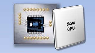
the heart of absolutely any Computing device be it personal computer smartphone or a programmable calculator is the center processor or CPU the cpu's main job is to execute programs or code what this actually means is that as soon as power is applied the processor hungry for executable code starts consuming data from external memory just like a person who reads a book word by word the processor reads the program by it by bite as long as power is applied to the Circuit the CPU cannot stop and program execution continues forever and just like a book is made up of sequence of letters words and sentences computer memory is organized as array of integer numbers called bytes and each byte can take a value from 0 to 255. in order for the CPU to know which memory cell exactly IT addresses all cells are numbered starting from zero the ordinal number of a cell is called address for example memory cell number 300 has an address of 299 that's because cell numbers start from zero computer memory is very similar to a sheet of paper you can write something in it that can be read later there are basically two types of memory read-only and random access read-only memory or ROM usually contains pre-programmed code which is intended for the CPU to execute while random access memory or ROM mostly contains temporary data either generated by the CPU itself or loaded by the CPU from external media during program execution as the name suggests read-only memory can only be read by the CPU while Random Access Memory can be both read and written to this means that ROM retains data even if you turn off your computer while Ram is erased every time Powers interrupted dim sticks installed in your PC or laptop is RAM and bios chip is wrong bios is a small program that is executed every time you boot up your system let's now take a glance at how it works imagine a very simple Computing device consisting of a CPU and a ROM chip the ROM chip contains a program called firmware the name firmware suggests that it's a proprietary piece of software that can only run on a certain device as the power is applied the CPU immediately addresses the ROM chip in an effort to read program code that it could execute obviously for that to happen it needs to read data from a number of memory cells so each cell is read by specifying its address which like was mentioned above is its unique ordinal number for the CPU to be able to tell the ROM chip the address of the cell it wants to read all computers have a communication system called address bus by Design it's basically a set of regular electrical wires that use binary system that's ones and zeros to encode memory cell address this method in fact is always used by computers to communicate numbers between devices imagine that the CPU wants to read cell whose address is 44 206. this is just a random sample number it doesn't mean anything let us now open Windows calculator and convert it to binary the result is this binary number note that it has 16 bits that's binary digits so exactly these ones and zeros the CPU will put up on the address bus to reach cell number 44 206.
yep it's that simple please note and that is very important the least significant bit LSB of the address which is zero in our case will be put up at address line a0 well the most significant bit MSB will be at line a15 address numbering like everything in programming also starts at zero because the address is always sent from the CPU to external devices and never in the reverse Direction the address bus is unidirectional which means the CPU address lines are outputs and the ROM chips address pins are inputs so all devices on a computer motherboard are connected to the address bus in parallel but it's obvious that computer memory supports two types of communication reading and writing how would the memory chip know which operation exactly the CPU intends to perform for that computers use a signaling system called the control bus it also consists of regular wires and its two most important lines are read and write designated as Rd and WR please note both the read and write signals are active low meaning if the CPU intends to perform a read operation it pulls the read line low if it wants to write data it pulls the right line low these two signals are mutually exclusive because it's not possible to read and write simultaneously the reason why I read and write and other control signals are active low is power consumption considerations okay so the CPU outputs the binary value of 44 206 to the address bus now to let the ROM chip know it intends to read the contents of this memory cell it also activates the read line you might wonder now why would the ROM chip need the read signal if read is all it can do and the CPU cannot write anything to it well thing is the CPU has no idea what type of memory it's addressing actually doesn't care so every time it wants to read something no matter if it's ROM or Ram it's reading from it will always pull the ridline low and in fact the ROM chip does need the read signal because it needs to know when exactly it's supposed to send the data requested to the CPU looks like now we need a mechanism to transfer data and here comes to play the data bus probably the most important and also complicated communication system in a computer and it's bi-directional in our example the data bus carries exactly eight bits of data because the size of the data bus directly affects the performance of the entire system it is precisely this that we mean when we say for example that the computer is 8-bit and the game console is 16-bit and the version of Windows is 32 or 64-bit in response to the cpu's request the ROM chip puts the contents of the memory cell located at address 44206 onto the data bus let's say the value is 112. naturally the data will also be presented in binary format 112 will look like this while the read operation is in progress the CPU becomes the receiving side and its data bus lines act as inputs and the ROM chips data bus pins act as outputs our little computer here has an 8-bit data bus which means the size always single memory cell is one byte which is exactly 8 Bits so our CPU has read exactly one byte of data and its value equals 112. like I said before the ROM chip contains firmware a computer programming machine code written by a programmer so 112 which is again just a sample value I picked is the command that tells the CPU to perform a certain task these commands are also called operation codes opcodes or machine code instructions so imagine it's the instruction to write a value of 205 to the memory cell located at address 62 088 please allow me to add a ram chip to write to to our improvised computer it will be connected in parallel to both the address and the data bus of our system like I said the address bus is unidirectional and in theory we can connect an infinite number of devices to it but now we got a problem when the CPU initiates a read or write operation because we now got two memory chips in our system how would they know which one the CPU is addressing if both of them get activated simultaneously their outputs will struggle and we're going to have a collision on our data bus here another very important mechanism in computer engineering comes into play it's called address decoding the term decoding here has nothing to do with ciphering or encryption it's merely a set of logic gates that output logic 0 whenever a certain pattern of ones and zeros is present on its inputs what exactly this combination should be is determined by the Circuit of the decoder itself so in order for the CPU to know exactly which device it's addressing when designing a computer system all address space is divided into ranges some part of it is taken by Rome another part by Ram imagine a book that has several chapters we know exactly which page each chapter starts and ends in and it's impossible to move chapters if the book had already been printed same thing happens in a computer's address space each memory device is assigned a certain address range which is fixed and cannot be altered the size of the entire address space is determined by the number of address bus lines and is always tied to the CPU model our computer here has a CPU with 16 address lines so the maximum number of bytes the CPU can address is 2 to the power of 16.
which is 65 536 bytes or 64 kilobytes you can also come up with this number using Windows calculator 16 binary Ones Will yield a decimal value of 65 535 because memory cell number one mind you as the address 0 not 1. so the address space of our computer starts at byte number zero and NZ byte number 65 535 and the total number of bytes that can be addressed is 65 536. for the CPU to be able to work both with ROM and RAM we need to wire them in such a way that they're activated whenever accessing the address range that is assigned to each of them based on our concept or we can say these two chips must be properly decoded to keep things simple in our little experiment each chip will have exactly half the memory space which is 32 kilobytes a piece ROM will take the lower 32k and RAM the upper 32k so the ROM will be located in the address range from 0 to 32 767 and Ram from 32 768 to 65 535.
why exactly like that and not the other way around ROM is usually placed at the start of the address space because that's where a typical CPU starts program execution after the reset signal arrives when you hit reset what you actually do is zero the program counter PC so address 0 is where the very first firmware instruction must be located all data between the CPU and memory chips will naturally be transferred in binary format here's what it's going to look like to be honest these numbers do not really fit well with the ear and are pretty hard to perceive so in computers and programming a hexadecimal numbering system is used it differs from decimal system and that in addition to digits from 0 to 9 Latin letters from A to F are used that also act as digits so hexadecimal uses a total of 16 digits instead of 10. in essence the hexadecimal system is a simplified way of representing binary numbers it basically boils down to a simple replacement of every combination of four binary digits there are also 16 of them with one hexadecimal digit like this so 8-bit of binary data can be represented by two hex digits while 16 bit of binary data will take up four hex digits and so on by the way in programming four bits are called a nibble 8 Bits are called a byte and 16 bits and up are called a word now these values will look like this and our ROM chip will decode to addresses from 0 to 7 FFF while the ram chip will take up address range from 8000 to ffff we must pronounce hex numbers by a single digit because 8000 is not 8 000. it's a different number hex numbers have their own designation and programming for example the C language uses prefix Ox while in Assembly Language Latin letter H H for hex uppercase or lowercase doesn't matter is appended at the end of the number all these designations are equivalent okay let us take a close look at these values and try to figure out how they differ in terms of address Buzz bits their binary representation tells us that their distinct difference is their most significant bit any HEX number in the range above 7ff has the highest address line that's a15 equal to 1.
any HEX number below 800 has address line a15 equal to zero so we need the ROM chip to activate when a15 is low and RAM chip to activate when a15 is high memory chips have a special control line for Activation called CS chip select or C chip enable which is basically the same the Cs signal is also active low if the IC is not active its outputs will be in the so-called z-state High impedance which means that the pin is effectively disconnected such outputs are also called Tri-State memory ICS also have the OE control signal which stands for output enable since ROM can only send data the Cs and oeither have basically the same meaning but for Ram active OE means the data is being read from the memory so to decode these two memory ICS all we have to do is use a simple inverter gate the ROM c signal will be wired directly to the a15 address line and ram C will be fed from the inverter the read signal will be wired to the output enable pins of both chips while the right signal will go to the right enable input of the ram chip the right signal is not used with the wrong chip naturally before us ladies and gentlemen is the real working Circuit of the simplest computer so how does it work once the CPU is reset its address pointer the program counter PC is zeroed so all address lines are set to logic 0.
Related Videos

36:37
How does USB work?
Ron Mattino
64,575 views

18:20
Transistors Explained - How transistors work
The Engineering Mindset
19,284,643 views
20:42
How a CPU Works
In One Lesson
8,402,343 views

28:30
How do Graphics Cards Work? Exploring GPU...
Branch Education
4,701,917 views

9:27
Quantum Spectrum SDR & Quantum View IP I...
HAMTech RADIO SCANNER M0FXB CB DRONE HOBBY Diary
20 views

42:32
How a Computer Works - from silicon to apps
Improbable Matter
1,752,228 views

20:11
But, what is Virtual Memory?
Tech With Nikola
411,791 views

36:31
How does NE555 work? Bistable, Monostable...
Ron Mattino
17,513 views

17:55
How do SSDs Work? | How does your Smartpho...
Branch Education
6,064,374 views

18:58
Architecture All Access: Modern CPU Archit...
Intel Technology
266,399 views

18:12
Exploring How Computers Work
Sebastian Lague
3,793,763 views

35:33
How does Computer Memory Work? 💻🛠
Branch Education
4,635,107 views

22:11
HAL 9000 and the Sexadecimal Mystery - Fin...
Dave's Garage
418,419 views

20:05
How a Clever 1960s Memory Trick Changed Co...
LaurieWired
481,514 views

14:28
HOW TRANSISTORS RUN CODE?
Core Dumped
866,569 views

27:25
“Hello, world” from scratch on a 6502 — Pa...
Ben Eater
5,201,822 views
14:22
How TRANSISTORS do MATH
In One Lesson
2,211,510 views

15:42
RAM Explained - Random Access Memory
PowerCert Animated Videos
3,176,355 views

19:49
CRAFTING A CPU TO RUN PROGRAMS
Core Dumped
210,387 views

18:09
Capacitors are terrible at remembering dat...
Core Dumped
147,467 views