Designing a Lag Compensator with Bode Plot
199.8k views2535 WordsCopy TextShare

Brian Douglas
Get the map of control theory: https://www.redbubble.com/shop/ap/55089837
Download eBook on the fund...
Video Transcript:
welcome back to control system lectures in this video let's talk about designing a lag compensator using a bod plot this video is a continuation of the series on designing lead and lag compensators if you haven't watched the previous videos I've put a link to the playlist in the description below where you can find the rest I recommend that you haven't already watched them you should start there and then this video will make a lot more sense in the video on designing a lead compensator using a bod plot I walked through a simple design problem where
we had a system with a plant of 1 /2s + 1 and we needed to design a control system that gave us less than 2% steady state error for a ramp input and the system had to have more than 48 Dees of phase margin the first two steps for Designing the lead compensator were actually generic steps that we're still going to take when designing a lag compensator so I'm going to repeat them quickly here the first step is to determine if the system type is sufficient to meet your steady state error requirement in our case
since we have a finite steady state error requirement to a ramp input we need a type one system or at least a single pole at the origin so we added that integrator 1 / s to our compensator without this increase in system type no amount of gain would ever allow us to meet our steady state error for a ramp input the error would continue to grow to infinity and that's because our system is only a type zero since there's no poles at the origin now let me draw our block diagram of our system so you
have a visualization of what we're trying to do we have our plant and now we've just added a 1/ s to increase the system type and that's part of our compensation and now that our system is capable of meeting our steady state error requirement step two is to choose a gain that's going to get us there and if you recall back to the other video we came up with K must be greater than 49 and to make the math easier we just chose k equals 50 so after our first two steps this is what our
system looks like and if we were to implement this controller 50 overs and close the loop we would meet our steady state error requirement but at this point we've done nothing to meet our phase margin requirement which brings us to step three where we drew the bod plot of our open loop system and our currently designed compensator to see how much phase margin we actually have so this is the open loop bod plot of our system it's 50 /2 s^2 + S and we find that we still only have our 18° of phase margin which
isn't enough to meet our requirement now in the last video we added a lead compensator to increase the phase margin and the philosophy behind that design was to add phase to the system where you want it without adjusting the gain at the point by too much which is exactly what we did and we came up with a lead compensator that looked like this we had a zero around min-1 and a pole around minus 45 but this is where I'm going to blow your mind what if I told you that we could still meet our phase
margin requirement by designing a lag compensator rather than a lead compensator essentially we'd just be taking this pole in zero and swapping them of course we can't just swap them in their current place there's a slightly different philosophy when using a lag compensator and that's because if we just had them trade places we'd be subtracting all of that phase right at that critical point instead of adding it and we'd actually be making our system less stable when using a lag compensator we're trying to meet our phase margin not by adjusting the phase but by adjusting
the magnitude plot you can clearly see that if we dropped magnitude the gain crossover frequency would move to the left which would increase our phase margin since phase gets further away from minus 180° as you go further left now we can reduce magnitude by just reducing the gain of the system but there is a problem with that we've already set the gain of the system to meet our steady state error requirements which is determined by this low frequency region in the bod plot so how can we maintain the same low frequency gain while still reducing
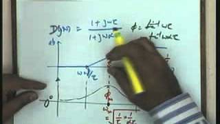
the gain at the critical region all while not disturbing the phase plot too much and that is with a lag compensator let's draw the bod plot for a lag compensator and see how this is accomplished here's an arbitrary lag compensator 2 s + 1 / 4S + 1 and its corresponding bod plot notice that when s approaches zero or Omega gets closer and closer to zero the magnitude of this lag compensator approaches 1 / 1 which is 0 DB and you can see that clearly on the graph that at low frequencies the magnitude is z
DB and we want the DC gain to be Zer DB since we've already stated that we don't want to mess up our steady state error so this won't affect it also as s approaches Infinity the magnitude approaches 2 / 4 or .5 which corresponds to- 6 DB and again we see that clearly in the bod plot it's this Unity gain at low frequency and attenuation at high frequency that is exactly what we're looking for in our design problem Oh a real quick side note this lag compensator has a zero at minus5 and a pole at
minus .25 but that doesn't mean that you can write the lag compensator as s plus5 / s +25 sure both of these have a single pole and single zero in the exact same place but their gain is different with this second method as s approaches zero the gain approaches 2 or 6 DB and as s approaches Infinity the gain approaches zero so essentially we've just increased the gain plot up by a factor of two or 6db and this is obvious when you try to do the math to convert from one to the other multiply the
numerator by 2 over two and the denominator by 4 over4 and we're left with our mysterious gain of two because if you leave out this two ID four you're effectively doubling the magnitude of the system so I'm going to stick with the first way that I wrote it because I think that it's cleaner but you can write it either way as long as you keep track of the gain okay now remember that our goal is to reduce the gain in the system but without affecting the phase too much and looking at the B plot of
the lag compensator it should be fairly obvious which frequency section will accomplish that it's this section that's the higher frequency off to the right up here you get large negative gain and relatively zero phase shift so when we choose the locations of the pole in zero we want to do so in such a way as to put this section of the lag compensator over the region of our system's B plot that we're trying to adjust and we do that by pushing this large phase lag portion to as low a frequency as we can handle okay
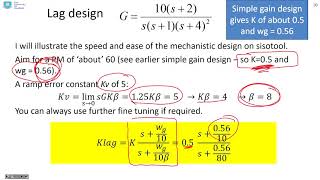
let's get back to designing the lag compensator to meet our phase margin requirement for our particular system here's the bod plot of our compensated open loop system again we only have 18 degrees of phase margin and we need at least 48° so step three of our lag compensator design is to determine at which frequency the phase would meet our phase margin requirement and then figure out what the gain is at that frequency so that you can determine how much you need to drop the gain by in order to make that the new gain crossover frequency
in our case it's about 18 DB but since the lag compensator doesn't add exactly zero phase shift and exactly the magnitude we want then it's usually a good idea to add a small safety factor to our phase margin so I'll drop the gain by 20 DB or a factor of exactly 10 this also has the added benefit of making the math easier for this video in your projects you might have to try a couple of factors before you settle on the one that you like best and if we look back at our lag bod plot
from above the gain is reduced at high frequencies by a factor that is equal to the ratio of these two numbers the numerator and the denominator so in order to drop the gain by a factor of 10 I need the lower number to be 10 times larger than the upper number so that sets the relative ratio between the two so how do we pick where to place the pole in the zero now that we know that the relative ratio between the two needs to be 1 over 10 well remember that we want our negative phase
lag to be as far left as possible which means placing the zero and pole as close to the imaginary axis as you can or making the number to as large as you possibly can the larger you can make this number the less the lag compensator will interfere with your original system remember this is the same philosophy we used when placing the pole in zero in describing how we designed a lag compensator with root Locus always as close to the origin as possible and just like before there is a limit to how close you can move
it because you start to get to a region that is physically impossible or at least really difficult to make in real life so the rule of thumb is to place the zero about 50 times closer to the origin as the dominant poles so in our case it would be 50 * 2 which is 10 so it' be 10 s + 1 in the numerator and 100 S + 1 in the denominator and that completes our compensator design for this system we have our lag compensator plus the gain that lets us meet our steady state error
plus our integrator to increase the system type and of course we have our original plant for our system so these four blocks represent our open loop system of course we would feedback Unity gain uh on the output and compare it with a reference at the beginning to generate an error term and this would be our closed loop system and this closed loop system should meet all of our requirements but we can test that in mat lab so the first thing I'm going to do is Define the systems to our workspace and I'm going to start
with our partially compensated system which has the 50 overs but no lead and no lag compensator then I'll Define the lead compensator which uh we generated in the video before and finally I'll Define the lag compensator which we just created right now and now I'm going to plot the Bodi plot for our partially compensated system alongside with our lead and lag compensated system so that you can see the differences between all three now let me add a legend real quick but you can see that the blue line is our partially compensated one with 18° of
margin our green line is the lead compensated system and the red line is the lag compensated system and if you right click and select characteristics and then show all stability margins it'll show you the phase margins for all three systems and check this out notice that the original system has a phase margin of 18° like we thought but both the phase lead and phase lag compensated systems have about 50° of phase margin so they both meet our requirement the other thing you should notice is that at really low frequencies the DC gain hasn't changed for
any of them which means we haven't messed up our steady state error requirement but perhaps the most obvious is that the gain crossover frequency was increased for the lead and decreased for the lag compensator and the gain crossover frequency is related to the speed of a control system so essentially we've slowed down the entire system so that it no long reacts as quickly and this will be obvious if I plot the step response to each of the closed loop systems first though I have to generate the closed loop system in mat lab using the feedback
command and then I can plot the step response for all three of them on top of each other similar to what I did with the B plot and there you go you can see all three systems the blue system which was the partially compensated one has only 18 degrees of phase margin so it's a little bit less stable than the other two but you'll notice that the green the lead compensated system not only is more stable but it's also fast and the lag compensated system is equally stable but a little bit slower pretty crazy huh
so now you might be saying well why the heck would we ever want to slow down our control system don't we want it to be as fast and awesome as possible well maybe but it depends on what your system is designed to do if your system doesn't need to react very quickly or you're not sending high frequency commands to it it's actually a better design to slow it down because then it won't react to high frequency noise as much and that'll make it a less noisy system also if your system has unknown or poorly modeled
highfrequency modes then by slowing down the system that model uncertainty won't affect you if your system isn't even able to respond to those high frequency modes so all in all both methods lead and lag have their benefits and drawbacks but by understanding them it'll help you decide which method you want to use when designing your control system now I hope you guys enjoyed this miniseries on designing a lead and lag compensator I'll try to use these techniques when designing controllers for my projects in the laboratory videos to give you some extra exposure to them if
you have any questions or comments please leave them below and I'll do my best to answer them don't forget to subscribe so you don't miss any future videos and as always thanks for watching
Related Videos
7:59
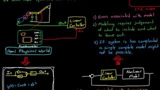
Modeling Physical Systems, An Overview
Brian Douglas
108,341 views
14:19
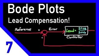
Designing a Lead Compensator with Bode Plot
Brian Douglas
368,024 views
26:58
A real control system - how to start desig...
Brian Douglas
278,466 views
13:58
Designing a Lead Compensator with Root Locus
Brian Douglas
484,649 views

11:16
Designing a Lag Compensator with Root Locus
Brian Douglas
206,178 views
13:20
What Is Robust Control? | Robust Control, ...
MATLAB
120,079 views

6:09
Weekend Update: Christmas Joke Swap 2024 -...
Saturday Night Live
4,350,568 views
13:54
Gain and Phase Margins Explained!
Brian Douglas
661,989 views
16:40
Nyquist Stability Criterion, Part 1
Brian Douglas
1,032,326 views

11:00
What are Lead Lag Compensators? An Introdu...
Brian Douglas
406,632 views
28:48
Example: Design Lead-Lag Controller
The Ryder Project
99,407 views
26:15
Tutorial on Step-by-Step Design of PHASE L...
Aleksandar Haber PhD
4,903 views
21:04
Design and Implementation of Controllers u...
KnowHow
20,545 views
56:53
Lec-41 Compensator Design Using Frequency ...
nptelhrd
77,315 views

13:38
Bode Plots by Hand: Real Poles or Zeros
Brian Douglas
367,802 views

12:21
What's a Tensor?
Dan Fleisch
3,769,305 views

11:36
Stability of Closed Loop Control Systems
Brian Douglas
257,063 views
33:00
Example: Design PID Controller
The Ryder Project
108,824 views
23:55
Lead and lag compensation using Bode diagrams
John Rossiter
12,022 views
24:28
Bode Plot Example
Electrical Engineering Topics
488,217 views